abse/dual-usb-peltier-assembly
A USB‑C PD Peltier controller PCB combining RP2040 control, adjustable buck‑boost TEC power, temperature sensing, fan regulation, USB programming, protection, status LEDs, and external accessory hardware.
- Version
- 0.4.6
- License
- unset
- Stars
- 0
src/parts/C20526.tsx
// Preserve the exact JLC catalog identity, including the 100–300 gain bin.
// Datasheet review: imported copper geometry corrected in place; explicit mask +0.05 mm and controlled paste.
// Exact EasyEDA/JLCPCB C20526; observed 2026-10-10T03:20:57.600274+00:00. Source: https://jlcsearch.tscircuit.com/api/easyeda_components/C20526
import type { ChipProps } from "@tscircuit/props"

const pinLabels = {
  pin1: ["B"],
  pin2: ["E"],
  pin3: ["C"]
} as const

export const MMBT3904_RANGE_100_300_ = (props: ChipProps<typeof pinLabels>) => {
  return (
    <transistor type="npn"
      pinLabels={pinLabels}
      symbol={
        <symbol>
          <port name="pin3" pinNumber={3} aliases={["C"]} direction="up" schX={0.2} schY={0.4} schStemLength={0.2} />
          <port name="pin1" pinNumber={1} aliases={["B"]} direction="left" schX={-0.2} schY={0} schStemLength={0.2} />
          <port name="pin2" pinNumber={2} aliases={["E"]} direction="down" schX={0.2} schY={-0.4} schStemLength={0.2} />
          <schematicpath points={[{"x":0.2,"y":0.2},{"x":0,"y":0.06}]} strokeColor="#880000" />
          <schematicpath points={[{"x":0,"y":-0.06},{"x":0.2,"y":-0.2}]} strokeColor="#880000" />
          <schematicpath points={[{"x":0,"y":0.18},{"x":0,"y":-0.18}]} strokeColor="#880000" />
          <schematicpath points={[{"x":0.2,"y":-0.2},{"x":0.14,"y":-0.1},{"x":0.08,"y":-0.18},{"x":0.2,"y":-0.2}]} strokeColor="#880000" isFilled fillColor="#880000" />
          <schematictext schX={0} schY={0.64} text="{NAME}" fontSize={0.2} anchor="bottom_center" />
        </symbol>
      }
      supplierPartNumbers={{
  "jlcpcb": [
    "C20526"
  ]
}}
      manufacturerPartNumber="MMBT3904(RANGE:100-300)"
      footprint={<footprint>
        <smtpad solderMaskMargin="0.05mm" solderPasteMargin={0} portHints={["pin1"]} pcbX="1.01mm" pcbY="-0.95mm" width="0.8mm" height="0.6mm" shape="rect" />
<smtpad solderMaskMargin="0.05mm" solderPasteMargin={0} portHints={["pin2"]} pcbX="1.01mm" pcbY="0.95mm" width="0.8mm" height="0.6mm" shape="rect" />
<smtpad solderMaskMargin="0.05mm" solderPasteMargin={0} portHints={["pin3"]} pcbX="-1.01mm" pcbY="0mm" width="0.8mm" height="0.6mm" shape="rect" />
<silkscreenpath strokeWidth="0.15mm" route={[{"x":0.726211400000011,"y":1.65},{"x":-0.726211400000011,"y":1.65},{"x":-0.726211400000011,"y":0.7}]} />
<silkscreenpath strokeWidth="0.15mm" route={[{"x":0.726211400000011,"y":-1.65},{"x":-0.726211400000011,"y":-1.65},{"x":-0.726211400000011,"y":-0.7}]} />
<silkscreencircle pcbX="0mm" pcbY="-0.95mm" radius="0.075mm" strokeWidth="0.15mm" />
<courtyardoutline outline={[{"x":-1.75,"y":1.75},{"x":1.75,"y":1.75},{"x":1.75,"y":-1.75},{"x":-1.75,"y":-1.75},{"x":-1.75,"y":1.75}]} />
      </footprint>}
      cadModel={{
        objUrl: "https://modelcdn.tscircuit.com/easyeda_models/assets/C20526.obj?uuid=d777607a152f4f3aac9bb0d0c14ed6fd",
        stepUrl: "https://modelcdn.tscircuit.com/easyeda_models/assets/C20526.step?uuid=d777607a152f4f3aac9bb0d0c14ed6fd",
        pcbRotationOffset: 180,
        modelOriginPosition: { x: 0.000012700000070253736, y: -0.000012699999956566899, z: 0.050795 },
      }}
      {...props}
    />
  )
}
Related Packages
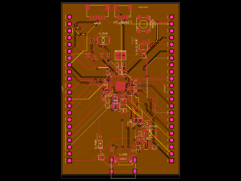 More from this authorabse/rp2350-mcu-boardThis code defines a compact, four-layer PCB hardware layout for the Raspberry Pi RP2350A microcontroller module, including the main IC, power regulation, USB-C connector, STM32-compatible headers, and associated passive components, with detailed component footprints, net connections, and copper pour zones for powering and ground references.
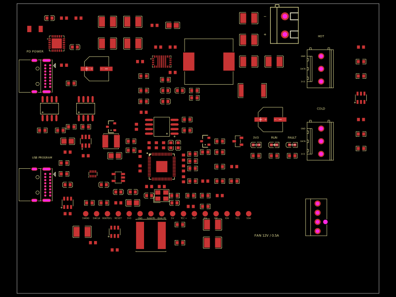 Similar package0hmX/dual-usb-peltier-assemblyA USB-C PD Peltier controller board featuring an RP2040, adjustable buck-boost TEC driver, temperature-sensor inputs, fan regulator, USB programming, protection, status LEDs, and supporting passives/connectors.
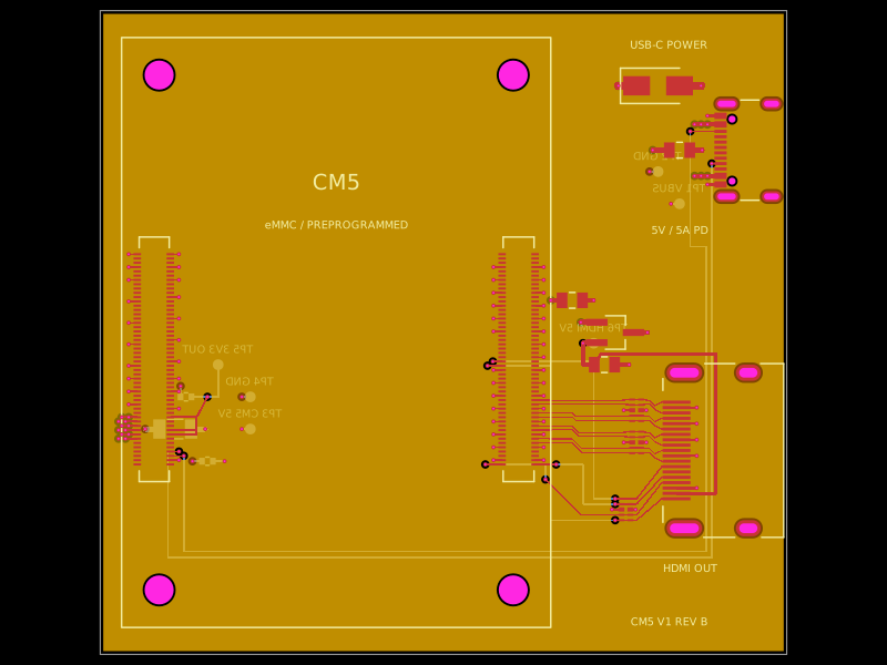 Discover something newpixalynx/cm5-minimal-carrierA 4-layer Raspberry Pi CM5 carrier board routes USB‑C 5V power through an RT9742 load switch with TVS protection and capacitive filtering, while providing ESD-protected HDMI output, CM5 connectors, test points, and ground/power planes.