AnasSarkiz/muse-voice-remote
Muse Voice Remote — bare ESP32-S3R8, 155 TOP JLCPCB parts with real supplier CAD, native 3D assembly and GLB exports. Revised 17 mm case allocation; 0.30 mm via drill /0.45 mm pad. Checked prototype PCB; mechanical, RF and MUSE qualification pending.
- Version
- 1.3.2
- License
- unset
- Stars
- 0
scripts/chip_native.py
"""Seed short RF/clock paths and a continuous inner ground reference.

Footprints and pads come from the retained JLCPCB imports. This adds board
copper, not component geometry. RF impedance and matching need fab/VNA review.
"""
import pcbnew


def seed_chip_copper(board, nets):
    footprints = {f.GetReference(): f for f in board.GetFootprints()}
    if footprints["U1"].GetValue() != "ESP32-S3R8":
        return

    def at(ref, number):
        p = next(p for p in footprints[ref].Pads() if p.GetNumber() == str(number))
        return (pcbnew.ToMM(p.GetPosition().x), pcbnew.ToMM(p.GetPosition().y))

    def path(net, points, width):
        for a, b in zip(points, points[1:]):
            if a == b:
                continue
            t = pcbnew.PCB_TRACK(board)
            t.SetStart(pcbnew.VECTOR2I(pcbnew.FromMM(a[0]), pcbnew.FromMM(a[1])))
            t.SetEnd(pcbnew.VECTOR2I(pcbnew.FromMM(b[0]), pcbnew.FromMM(b[1])))
            t.SetLayer(pcbnew.F_Cu)
            t.SetWidth(pcbnew.FromMM(width))
            t.SetNet(nets[net])
            t.SetLocked(True)
            board.Add(t)

    # RF stays on the top layer, with no RF signal vias or meanders. These
    # widths are design targets; the fabrication stackup must establish 50 ohm.
    path("RF_LNA", [at("L_RF_MATCH", 2), at("C_RF_LNA", 1), at("U1", 1)], 0.18)
    path("RF_3V3", [at("U1",2),at("U1",3)],0.2)
    # The connector's signal exits south of its two large shield lands.
    path("RF_ANT", [at("J_RF", 2), (-12.7,-4.3), (-12.7,-3.8), (-11.0,-3.8),
                    (-10.5,-4.3), (-10.5,at("D_RF_ESD",1)[1]), at("D_RF_ESD", 1),
                    at("C_RF_ANT", 1), at("L_RF_MATCH", 1)], 0.18)
    path("XTAL_P_CHIP", [at("U1", 54), at("L_XTAL", 1)], 0.15)
    path("XTAL_P", [at("L_XTAL", 2), (-1.8, -8.0), (-1.1, -8.7), at("Y1", 1)], 0.15)
    path("XTAL_P", [at("Y1", 1), (-3.0, at("Y1", 1)[1]), at("C_XTAL_P", 1)], 0.15)
    path("XTAL_N", [at("U1", 53), (-1.4, -6.25), (-0.8, -6.85), (2.4, -6.85), (2.4, at("Y1", 3)[1]), at("Y1", 3)], 0.15)
    path("XTAL_N", [(2.4, at("C_XTAL_N", 1)[1]), at("C_XTAL_N", 1)], 0.15)

    plane = pcbnew.ZONE(board)
    plane.SetLayer(pcbnew.In1_Cu)
    plane.SetNet(nets["GND"])
    plane.SetLocalClearance(pcbnew.FromMM(0.15))
    plane.SetMinThickness(pcbnew.FromMM(0.15))
    plane.SetPadConnection(pcbnew.ZONE_CONNECTION_FULL)
    outline = plane.Outline()
    outline.NewOutline()
    for x, y in [(-32.4,-23.4),(32.4,-23.4),(32.4,23.4),(-32.4,23.4)]:
        outline.Append(pcbnew.FromMM(x), pcbnew.FromMM(y))
    board.Add(plane)
    # Fill from a reloaded board/project in a separate process. KiCad 9's
    # zone filler crashes on freshly constructed boards without project state.
Related Packages
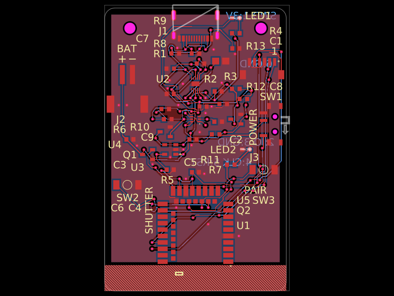 More from this authorAnasSarkiz/magnetic-shutter-remote--01a0f81fA compact USB‑C rechargeable battery device with BQ25185 charging, 3.3‑V regulation and protection, E73 Bluetooth control, temperature monitoring, status/charge LEDs, shutter/pair/power switches, and a mechanically enclosed Li‑Po battery with docking/antenna provisions.
 Similar packagemohan-bee/esp32-c3This hardware design integrates an ESP32-C3 microcontroller, a USB-C connector, a power management IC (AP2112-3.3V regulator), a USB-to-Serial converter (CH340C), several resistors, capacitors, and user-accessible headers to facilitate USB communication, power regulation, and general I/O interfacing.
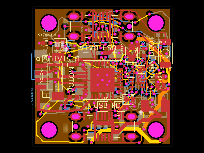 Discover something newShiboSoftwareDev/nema8-20mm-dual-usbc-stepper-controllerA compact 20 mm four-layer USB‑C stepper-controller PCB combining CH32X035 MCU control, TMC2209 motor driving, USB‑C PD/data interfaces, protection/power regulation, temperature/LED status hardware, and NEMA8 motor connectivity.