AnasSarkiz/muse-voice-remote
Muse Voice Remote — bare ESP32-S3R8, 155 TOP JLCPCB parts with real supplier CAD, native 3D assembly and GLB exports. Revised 17 mm case allocation; 0.30 mm via drill /0.45 mm pad. Checked prototype PCB; mechanical, RF and MUSE qualification pending.
- Version
- 1.3.2
- License
- unset
- Stars
- 0
docs/lcd-interface.md
# ER-TFT028A2-4 electrical integration

The exact 24-page EastRising manufacturer PDF v1.0 (2019-12-02) was downloaded from the public reference at https://github.com/sndsgd/kicad-er-tft028a2-4. Its title, panel model and outline dimensions match the requested display and assembly study. The original manufacturer endpoint still returns a Cloudflare challenge. The retained PDF and SHA-256/source records are in `docs/datasheets/ER-TFT028A2-4.pdf` and `docs/datasheets/download-results.json`. A public mirror is a document source, not a manufacturer endorsement or proof of current panel stock.

The panel requires a **50-pin, 0.5 mm, top-contact ZIF** connector (p.5). Selected Hirose **FH12A-50S-0.5SH(55)** (JLCPCB **C202120**) has positive exact JLCPCB stock, a retained manufacturer drawing and its imported JLCPCB footprint. The original TE connector was out of stock in the JLCPCB catalog. Its nominal 0.30 mm cable thickness agrees with the panel stiffener specification. Pin numbering/contact orientation must still be checked against the actual folded FPC and connector drawing during mechanical fit qualification.

## Pin assignment

Pin table and interface straps follow manufacturer pp.9–10, using four-wire, eight-bit serial interface **II**: IM3..IM0 = **1110**. GPIO signals pass through five SN74LVC1G125 buffers powered from 2.8 V, preserving the panel input limit VIH ≤ VDDI. TLV70228DBVR supplies the 2.8 V logic/analog rail from 3.3 V with local capacitors.

| FPC pins | Connection |
| --- | --- |
| 1 | LEDK directly to BL_SENSE and 5.1 Ω feedback resistor |
| 2–5 | Four individual anodes, each through 100 Ω ballast from boost output |
| 6 / 7 / 8 / 9 | IM0 ground / IM1 high / IM2 high / IM3 high |
| 10 | Reset from GPIO47 through 2.8 V buffer |
| 11–14 | Unused RGB timing inputs held at ground |
| 15–32 | Unused parallel DB17..DB0 inputs held at ground |
| 33 | SDO unconnected; write-only SPI |
| 34 | SDI from GPIO16 through 2.8 V buffer |
| 35 | Unused parallel RD held high at 2.8 V |
| 36 | D/C from GPIO21 through 2.8 V buffer |
| 37 | SCL from GPIO17 through 2.8 V buffer |
| 38 | CS from GPIO18 through 2.8 V buffer |
| 39 | TE output unconnected |
| 40–42 | VDDI/VDDI/VCI at 2.8 V |
| 43, 48–50 | Ground |
| 44–47 | Touch pins unconnected for the no-touch panel |

The startup pulls keep reset low and CS high while the MCU pins are undriven. Initialization, reset/sleep timing, SPI clock and landscape MADCTL configuration still require validation against the ILI9341 controller documentation and actual panel. The panel is physically 240 × 320 and is requested as **320 × 240 landscape** through controller rotation. No LCD firmware is claimed to have run on hardware.

## Backlight

The manufacturer specifies four parallel LEDs, approximately 3.2 V typical / 3.4 V maximum at 80 mA total, with 70–80 mA array current (p.11). TPS61169 is supplied from regulated 3.3 V and provides a constant-current boost output through a 10 µH Coilcraft LPS4018 inductor and a 60 V SS16 diode. The output capacitor is a 50 V KEMET part, covering the driver's open-load protection range.

The 5.1 Ω, 1% feedback resistor sets **40 mA total nominal** from 204 mV feedback. The 220 mV datasheet maximum and resistor tolerance give 43.6 mA static worst case, below the panel's 80 mA maximum. Four 100 Ω ballast resistors improve current sharing and provide boost headroom. The brightness is deliberately below the manufacturer's 70–80 mA characterization point. Individual current balance, brightness, transients and thermal behavior require bench qualification.

GPIO48 drives the PWM control with a 1 kΩ default-low bias. GPIO42 drives an MMBT3904 gate transistor through 1 kΩ; a 1 kΩ base pull-down keeps it off at reset. The transistor switches the AO3401A PMOS gate; a 100 kΩ gate-to-source resistor holds the **low-voltage input switch** off. Its source is V3_3 and drain is BL_INPUT, supplying both TPS61169 VIN and the inductor. LEDK is connected directly to the feedback node. The selected PMOS therefore does not encounter the boost output voltage. This input isolation prevents the inductor/diode path from feeding the LEDs while off.

Firmware sequence: hold GPIO42 and PWM low at boot, establish/reset/initialize the panel, enable the input switch, then apply PWM. For hard-off, set PWM low and allow driver shutdown before removing BL_INPUT. A 5 ms guard is a proposed margin over the 2.5 ms typical shutdown timing, not a verified worst-case guarantee. The documented 5–100 kHz PWM range includes 20 kHz. Confirm sequencing and current at open-load, minimum supply and maximum supply on the prototype.

## Mechanical and release limits

The real connector has a much larger envelope than the old 7 × 12 mm allocation. It is placed vertically on PCB top at X=21.5 mm, Y=3.5 mm. Supporting components were moved using complete imported courtyards, including rectangular courtyards. The LCD flex fold, entry direction, latch opening, assembly sequence, pack clearance and actual tolerance stack still need supplier CAD/physical fit checks.

The LCD circuit is now present; the physical panel's live stock remains unverified because the vendor site is blocked. Protected battery/NTC, antenna/transducer fit, power/current widths, planes/USB/EMI/thermal behavior and MUSE integration remain separate release gates. No fabrication sign-off is implied by a clean connectivity/DRC result.
Related Packages
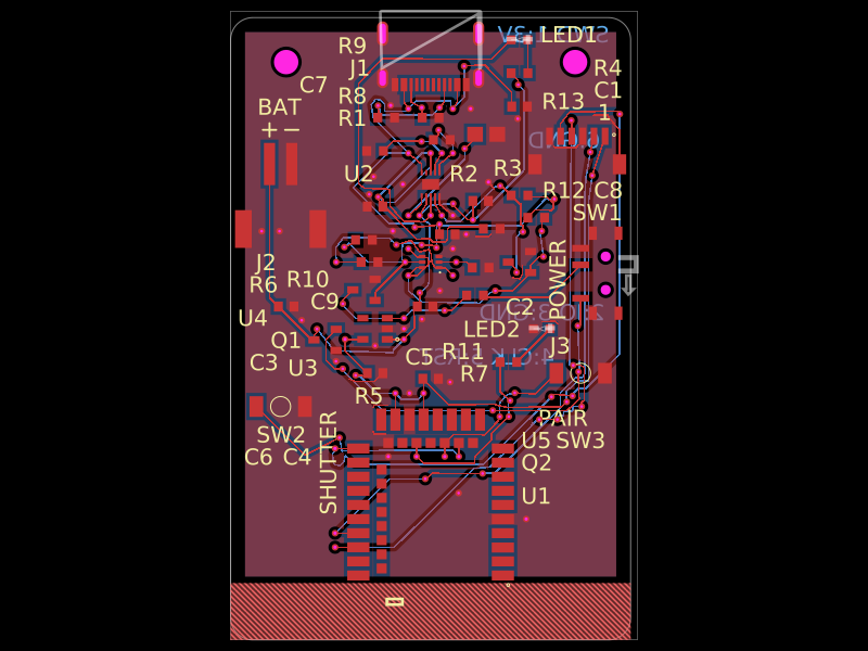 More from this authorAnasSarkiz/magnetic-shutter-remote--01a0f81fA compact USB‑C rechargeable battery device with BQ25185 charging, 3.3‑V regulation and protection, E73 Bluetooth control, temperature monitoring, status/charge LEDs, shutter/pair/power switches, and a mechanically enclosed Li‑Po battery with docking/antenna provisions.
 Similar packagemohan-bee/esp32-c3This hardware design integrates an ESP32-C3 microcontroller, a USB-C connector, a power management IC (AP2112-3.3V regulator), a USB-to-Serial converter (CH340C), several resistors, capacitors, and user-accessible headers to facilitate USB communication, power regulation, and general I/O interfacing.
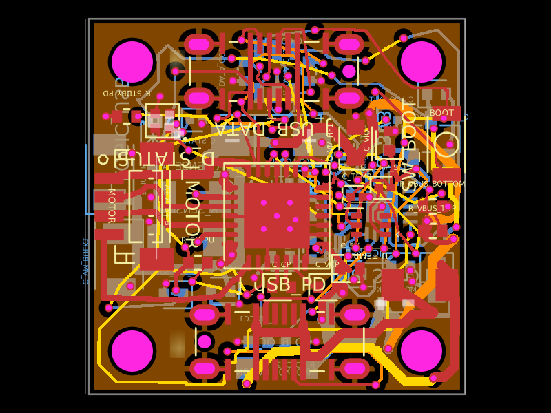 Discover something newShiboSoftwareDev/nema8-20mm-dual-usbc-stepper-controllerA compact 20 mm four-layer USB‑C stepper-controller PCB combining CH32X035 MCU control, TMC2209 motor driving, USB‑C PD/data interfaces, protection/power regulation, temperature/LED status hardware, and NEMA8 motor connectivity.