rushabhcodes/ESP32-E-Reader
A compact ESP32-C3 e-reader PCB integrating LiPo charging/protection, USB-C, 3.3 V regulation, e-paper display bias generation, microSD storage, and tactile controls.
- Version
- 1.0.85
- License
- unset
- Stars
- 3
index.circuit.tsx
PCB
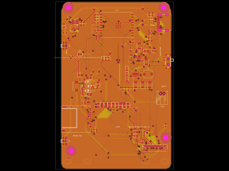
Schematic

/**
 * ESP32 E-Reader Rev. B
 *
 * Board-level composition. Electrical data and exact PCB placements live in
 * design-data.ts; functional blocks live in circuit-sections.tsx.
 */

import { Fragment } from "react";
import { assembly } from "tscircuit";
import { SparkFun_PRT_13855 } from "./imports/SparkFun_PRT_13855";
import antennaEnvelopeUrl from "./assets/enclosure/antenna-envelope-DO-NOT-PRINT.glb";
import batteryLinerUrl from "./assets/enclosure/battery-liner-DO-NOT-PRINT.glb";
import batteryAdhesiveUrl from "./assets/enclosure/battery-adhesive-DO-NOT-PRINT.glb";
import { Waveshare_3_97inch_ePaper_G } from "./imports/Waveshare_3_97inch_ePaper_G";
import displayConnection from "./assets/enclosure/display-connection.json";
import frontChassisUrl from "./assets/enclosure/front-chassis.glb";
import displayCushioningUrl from "./assets/enclosure/display-cushioning.glb";
import pcbCoverFastenersUrl from "./assets/enclosure/pcb-cover-fasteners.glb";
import rearCoverUrl from "./assets/enclosure/rear-cover.glb";
import pcbMounts from "./assets/enclosure/pcb-mounts.json";
import { CircuitSections } from "./circuit-sections";
import { nets, traceThicknessByNet } from "./design-data";
import { createPreExpansionAutorouter } from "./pre-expansion-autorouter";

// The compact tactile switches fit inside the display-width lower section.
const boardOutline = [
	{ x: -26.25, y: 48.08 },
	{ x: 26.25, y: 48.08 },
	{ x: 29.79, y: 46.62 },
	{ x: 31.25, y: 43.08 },
	{ x: 31.25, y: -44 },
	{ x: 30.37, y: -46.12 },
	{ x: 28.25, y: -47 },
	{ x: -28.25, y: -47 },
	{ x: -30.37, y: -46.12 },
	{ x: -31.25, y: -44 },
	{ x: -31.25, y: 43.08 },
	{ x: -29.79, y: 46.62 },
];

export function EReaderBoard() {
	return (
		<board
			title="ESP32 E-Reader Rev. B"
			width="62.5mm"
			height="95.08mm"
			outline={boardOutline}
			doubleSidedAssembly
			layers={4}
			thickness="1.6mm"
			minViaHoleDiameter="0.3mm"
			minViaPadDiameter="0.6mm"
			minViaEdgeToPadEdgeClearance="0.25mm"
			// Standard-cost through vias, with a 0.15 mm radial annulus.
			minViaHoleEdgeToViaHoleEdgeClearance="0.2mm"
			minPlatedHoleDrillEdgeToDrillEdgeClearance="0.45mm"
			minTraceToHoleEdgeClearance="0.2mm"
			minBoardEdgeClearance="0.3mm"
			minTraceToPadEdgeClearance="0.1mm"
			// Keep nearby schematic branches wired instead of replacing them with labels.
			schMaxTraceDistance={4}
			autorouter={{
				algorithmFn: createPreExpansionAutorouter,
				allowViaInPad: false,
			}}
		>
			{/* Four M2.5 screw points match the enclosure bosses and clamp both ends. */}
			{pcbMounts.mounts.map(({ name, x, y }) => (
				<Fragment key={name}>
					<hole diameter={pcbMounts.holeDiameter} pcbX={x} pcbY={y} />
					<keepout
						shape="circle"
						radius={pcbMounts.copperKeepoutRadius}
						pcbX={x}
						pcbY={y}
						layers={["top", "inner1", "inner2", "bottom"]}
					/>
				</Fragment>
			))}

			{/* Keep GND layer transitions clear of the nearby top-layer SPI clock. */}
			<keepout
				shape="circle"
				radius="0.25mm"
				pcbX={-0.35}
				pcbY={-8.34}
				layers={["inner2"]}
			/>
			{/* The RESE escape must not drill through J2's adjacent pin-3
			    contact. Keep its via clear of the connector pad on buried layers. */}
			<keepout
				shape="circle"
				radius="0.65mm"
				pcbX={displayConnection.connector.centerX + 4.75}
				pcbY={displayConnection.connector.centerY + 1.25}
				layers={["inner1", "inner2", "bottom"]}
			/>

			{/* Fine-pitch contacts must stay free of through-drills, including
			    vias on their own net. Top copper remains available for escapes. */}
			<keepout
				shape="rect"
				width="13mm"
				height="1.4mm"
				pcbX={displayConnection.connector.centerX}
				pcbY={displayConnection.connector.centerY + 1.250061}
				layers={["inner1", "inner2", "bottom"]}
			/>
			{/* Keep layer-transition pads clear of the C28 pin-2 edge. */}
			<keepout
				shape="rect"
				width="1.6mm"
				height="1.225mm"
				pcbX={-5.9}
				pcbY={-11.57}
				layers={["inner1", "inner2", "bottom"]}
			/>
			{/* Through vias span every copper layer, even when a route only
			    changes between buried layers. Protect the USB-C contact row. */}
			<keepout
				shape="rect"
				width="1.65mm"
				height="7.4mm"
				pcbX={23.811}
				pcbY={36.26}
				layers={["inner1", "inner2", "bottom"]}
			/>
			{/* Keep drills out of both contact rows on protection IC U3. */}
			{[-22.100304, -24.398496].map((x) => (
				<Fragment key={`protection-pad-via-clearance-${x}`}>
					<keepout
						shape="rect"
						width="1.6mm"
						height="2.95mm"
						pcbX={x}
						pcbY={36.6244}
						layers={["inner1", "inner2", "bottom"]}
					/>
				</Fragment>
			))}
			{/* C19/C20 ground pads must remain clear of display-signal vias. */}
			<keepout
				shape="rect"
				width="4.05mm"
				height="1.525mm"
				pcbX={3.525}
				pcbY={-9.745}
				layers={["inner1", "inner2", "bottom"]}
			/>

			<CircuitSections />

			{/* Route the display D/C and reset signals as explicit point-to-point
			    connections. The net-level autorouter split these two paths into
			    disconnected copper segments beside J2's fine-pitch contacts. */}
			<trace from={nets.EPD_DC[0]} to={nets.EPD_DC[1]} thickness="0.2mm" schDisplayLabel="EPD_DC" />
			<trace from={nets.EPD_RST[0]} to={nets.EPD_RST[1]} thickness="0.2mm" schDisplayLabel="EPD_RST" />
			<trace from={nets.EPD_RST[1]} to={nets.EPD_RST[2]} thickness="0.2mm" schDisplayLabel="EPD_RST" />
			{Object.entries(nets).filter(([name]) => !["EPD_DC", "EPD_RST"].includes(name)).map(([name, connections]) => (
				<Fragment key={name}>
					<net
						name={name}
						isGroundNet={name === "GND"}
						isPowerNet={["GND", "V3V3", "USB_VBUS", "BATT_P"].includes(name)}
					/>
					{connections.map((connection, index) => (
						<Fragment key={`${name}-${index}`}>
							<trace
								from={connection}
								to={`net.${name}`}
								thickness={traceThicknessByNet[name] ?? "0.2mm"}
							/>
						</Fragment>
					))}
				</Fragment>
			))}

			{/* Four-layer fills provide short returns and a dedicated 3.3 V plane. */}
			<copperpour
				name="GND_FILL_TOP"
				connectsTo="net.GND"
				layer="top"
				clearance="0.2mm"
				boardEdgeMargin="0.3mm"
			/>
			<copperpour
				name="GND_FILL_BOTTOM"
				connectsTo="net.GND"
				layer="bottom"
				clearance="0.2mm"
				boardEdgeMargin="0.3mm"
			/>
			<copperpour
				name="GND_PLANE_INNER1"
				connectsTo="net.GND"
				layer="inner1"
				clearance="0.2mm"
				boardEdgeMargin="0.3mm"
			/>
			<copperpour
				name="V3V3_PLANE_INNER2"
				connectsTo="net.V3V3"
				layer="inner2"
				clearance="0.2mm"
				boardEdgeMargin="0.3mm"
			/>

			<silkscreentext text="BATT" pcbX={27} pcbY={0} fontSize="1mm" />
			<silkscreentext
				text="USB"
				pcbX={27}
				pcbY={31}
				pcbRotation={90}
				fontSize="1mm"
			/>
			<silkscreentext
				text="WAKE"
				pcbX={-28}
				pcbY={20}
				pcbRotation={90}
				fontSize="1mm"
			/>
			<silkscreentext
				text="MAIN PWR"
				pcbX={25}
				pcbY={20}
				pcbRotation={90}
				fontSize="1mm"
			/>
			<silkscreentext
				text="EN"
				pcbX={-28}
				pcbY={-31}
				pcbRotation={90}
				fontSize="1mm"
			/>
			<silkscreentext text="EPD" pcbX={1} pcbY={-23} fontSize="1mm" />
			<silkscreentext text="MICRO SD" pcbX={-22} pcbY={-28} fontSize="1mm" />
			<silkscreentext
				text="ESP32 E-Reader  Rev. B"
				pcbX={13}
				pcbY={-23}
				fontSize="1mm"
			/>
		</board>
	);
}

export default function ESP32EReader() {
	return (
		<assembly.device name="ESP32_E_READER">
			<EReaderBoard />
			<Waveshare_3_97inch_ePaper_G />
			<SparkFun_PRT_13855 />
			<assembly.cadassembly
				name="wifi_antenna_envelope"
				cadModel={{ glbUrl: antennaEnvelopeUrl, modelUnitToMmScale: 1 }}
			/>
			<assembly.cadassembly
				name="front_chassis"
				cadModel={{
					glbUrl: frontChassisUrl,
					modelUnitToMmScale: 1,
					showAsTranslucentModel: true,
				}}
			/>
			<assembly.cadassembly
				name="display_cushioning"
				cadModel={{ glbUrl: displayCushioningUrl, modelUnitToMmScale: 1 }}
			/>
			<assembly.cadassembly
				name="battery_liner"
				cadModel={{ glbUrl: batteryLinerUrl, modelUnitToMmScale: 1 }}
			/>
			<assembly.cadassembly
				name="battery_adhesive"
				cadModel={{ glbUrl: batteryAdhesiveUrl, modelUnitToMmScale: 1 }}
			/>
			<assembly.cadassembly
				name="pcb_cover_fasteners"
				cadModel={{ glbUrl: pcbCoverFastenersUrl, modelUnitToMmScale: 1 }}
			/>
			<assembly.cadassembly
				name="rear_cover"
				cadModel={{
					glbUrl: rearCoverUrl,
					modelUnitToMmScale: 1,
					showAsTranslucentModel: true,
				}}
			/>
		</assembly.device>
	);
}
Related Packages
 More from this authorrushabhcodes/tetrisThis code defines various electronic component models—including a AAA battery holder, ATtiny85 microcontroller, switch, buzzer, display, and resistors—as hardware modules with detailed footprints, pin configurations, CAD models, and physical specifications for use in circuit design.
 Similar packagemohan-bee/esp32-c3This hardware design integrates an ESP32-C3 microcontroller, a USB-C connector, a power management IC (AP2112-3.3V regulator), a USB-to-Serial converter (CH340C), several resistors, capacitors, and user-accessible headers to facilitate USB communication, power regulation, and general I/O interfacing.
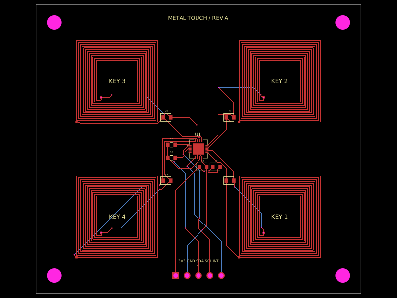 Discover something newhrithik18k/metal-touch-panelA PCB autorouting wrapper that corrects footprint-trace obstacle dimensions, solves routes with a preloaded trace-graph solver, and reports completed traces or routing errors.