proyectotictac/Conmutador-Transistor-NPN-mejorado
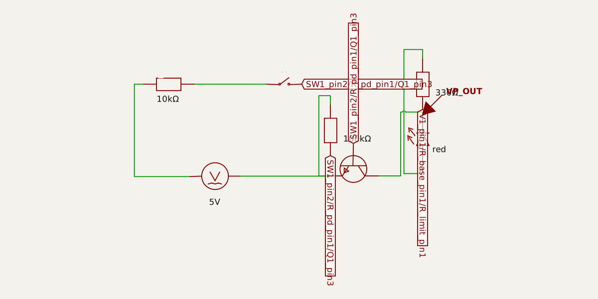
This circuit diagram models a transistor switch controlled by a push-button, with input and pull-down resistors, an LED indicator with current limiting resistor, and a voltage probe for monitoring, all powered by a 5V source.
- Version
- 0.0.1
- License
- unset
- Stars
- 0
index.tsx
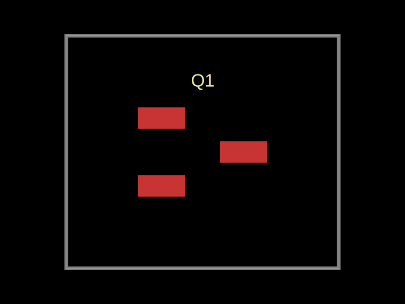
PCB
Schematic
export default () => (
  <board schMaxTraceDistance={10} routingDisabled>
    <voltagesource name="V1" voltage="5V" />

    {/* Resistencia de entrada y Switch */}
    <resistor name="R_base" resistance="10k" schX={-1} schY={2} />
    <switch name="SW1" simSwitchFrequency="1kHz" schX={1.5} schY={2} />

    {/* MEJORA 1: Resistencia de Pull-down (100k) para evitar ruido */}
    <resistor name="R_pd" resistance="100k" schX={2.5} schY={1} schRotation={90} />

    {/* Transistor NPN de Conmutación */}
    <transistor
      name="Q1"
      type="npn"
      footprint="sot23"
      schX={3}
      schY={0.3}
      schRotation={180}
    />

    {/* MEJORA 2: Carga visual (LED + Resistencia limitadora) */}
    <resistor name="R_limit" resistance="330" schX={4.5} schY={2} schRotation={90} />
    <led name="LED1" color="red" schX={4.5} schY={0.8} schRotation={90} />

    {/* Trazas del circuito de control */}
    <trace from=".V1 > .pin1" to=".R_base > .pin1" />
    <trace from=".R_base > .pin2" to=".SW1 > .pin1" />
    <trace from=".SW1 > .pin2" to=".Q1 > .base" />
    <trace from=".Q1 > .base" to=".R_pd > .pin1" />
    <trace from=".R_pd > .pin2" to=".V1 > .pin2" />

    {/* Trazas del circuito de carga */}
    <trace from=".V1 > .pin1" to=".R_limit > .pin1" />
    <trace from=".R_limit > .pin2" to=".LED1 > .anode" />
    <trace from=".LED1 > .cathode" to=".Q1 > .collector" />

    {/* Conexión a tierra (GND) */}
    <trace from=".Q1 > .emitter" to=".V1 > .pin2" />

    {/* Sonda para verificar la oscilación en el colector */}
    <voltageprobe name="VP_OUT" connectsTo=".LED1 > .cathode" />

    <analogsimulation duration="4ms" timePerStep="1us" spiceEngine="ngspice" />
  </board>
)