pixalynx/edge-connector
Configures USB-A, Micro-USB, and USB-C PCB-edge connectors with exposed copper contacts and automatically shaped, positioned board tongues.
- Version
- 1.0.0
- License
- GPL-3.0-only
- Stars
- 0
UsbAEdgeConnector.tsx
import type { ChipProps } from "tscircuit"
import { EdgeContactFootprint } from "./EdgeContactFootprint"

export const usbAEdgeConnectorPinLabels = {
  pin1: ["VBUS"],
  pin2: ["DM", "D_MINUS"],
  pin3: ["DP", "D_PLUS"],
  pin4: ["GND"],
} as const

/** Millimetres, relative to the component origin at pcbRotation={0}. */
export const usbAEdgeConnectorGeometry = {
  tongueWidth: 12,
  boardThickness: 2,
  tipY: 4.8,
  shoulderY: -3.9,
  edgeProfile: [
    { x: -6, y: -3.9 },
    { x: -6, y: 4.3 },
    { x: -5.5, y: 4.8 },
    { x: 5.5, y: 4.8 },
    { x: 6, y: 4.3 },
    { x: 6, y: -3.9 },
  ],
} as const

export type UsbAEdgeConnectorProps = Omit<
  ChipProps<typeof usbAEdgeConnectorPinLabels>,
  "footprint" | "pinLabels" | "layer" | "cadModel" | "children"
>

/**
 * USB 2.0 Type-A male PCB contacts. Top copper, insertion toward local +Y.
 * Looking down at the contacts with the tip up: VBUS, D-, D+, GND.
 * The host board must supply the tongue outline and thickness (see README).
 */
export function UsbAEdgeConnector(props: UsbAEdgeConnectorProps) {
  return (
    <connector
      schWidth={2.2}
      schHeight={1}
      schPinArrangement={{
        rightSide: { pins: [1, 2, 3, 4], direction: "top-to-bottom" },
      }}
      showPinAliases
      {...props}
      layer="top"
      doNotPlace
      pinLabels={usbAEdgeConnectorPinLabels}
      footprint={
        <EdgeContactFootprint
          solderMaskMargin={0.05}
          // USB-A-PCB reference geometry, rounded to 0.01 mm; see README.
          pads={[
            { pin: "pin1", x: -3.5, y: 0, width: 1.5, height: 7.5, layer: "top" },
            { pin: "pin2", x: -1, y: -0.5, width: 1, height: 6.5, layer: "top" },
            { pin: "pin3", x: 1, y: -0.5, width: 1, height: 6.5, layer: "top" },
            { pin: "pin4", x: 3.5, y: 0, width: 1.5, height: 7.5, layer: "top" },
          ]}
        />
      }
    />
  )
}

export default UsbAEdgeConnector
Related Packages
 More from this authorpixalynx/esp32-gps-cellular-trackerThis code defines a hardware layout comprising a Wi-Fi-enabled ESP32 module, GPS module, cellular GSM module, battery management components (including charger, protection circuits, and voltage regulators), USB-C connector, SIM card holder, RF components, and supporting passive components for a comprehensive GPS+Cellular tracker device.
 Similar packagemohan-bee/esp32-c3This hardware design integrates an ESP32-C3 microcontroller, a USB-C connector, a power management IC (AP2112-3.3V regulator), a USB-to-Serial converter (CH340C), several resistors, capacitors, and user-accessible headers to facilitate USB communication, power regulation, and general I/O interfacing.
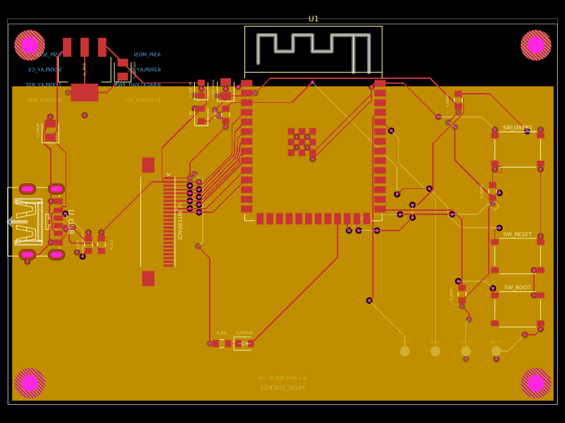 Discover something newShiboSoftwareDev/muse-m5stack-sticks3-replacementA 4-layer ESP32-S3 carrier board with USB-C 5V input, AMS1117 3.3V regulation, FFC interface, reset/boot/user buttons, status LED, and passives for compact display/control applications.