pixalynx/cm5-minimal-carrier
A 4-layer Raspberry Pi CM5 carrier board routes USB‑C 5V power through an RT9742 load switch with TVS protection and capacitive filtering, while providing ESD-protected HDMI output, CM5 connectors, test points, and ground/power planes.
- Version
- 0.1.1
- License
- unset
- Stars
- 0
scripts/package-review.py
"""Create inspection drawings and a checksummed, review-only manufacturing handoff."""
import csv, hashlib, html, json, pathlib, zipfile
R=pathlib.Path(__file__).resolve().parents[1];O=R/'output';G=O/'fabrication-REVIEW'
C=json.loads((R/'dist/index/circuit.json').read_text());D=json.loads((R/'lib/design.json').read_text());M=json.loads((R/'lib/manufacturing.json').read_text())
audit=json.loads((O/'manufacturing-audit.json').read_text())
for name,digest in audit['sha256'].items():
    assert hashlib.sha256((R/name).read_bytes()).hexdigest()==digest, 'Stale manufacturing audit: '+name
sc={p['source_component_id']:p['name'] for p in C if p['type']=='source_component'}
components={p['pcb_component_id']:p for p in C if p['type']=='pcb_component'}
by_ref={sc[p['source_component_id']]:p for p in components.values()}
def physical_pin(e):return next((p[3:] for p in e.get('port_hints',[]) if p.startswith('pin')),'')
def at(x,y,bottom=False):return ((32-x) if bottom else (x+32),30-y)
esc=html.escape
for bottom in [False,True]:
    layer='bottom' if bottom else 'top';label='BOTTOM — viewed from below (drawing mirrored)' if bottom else 'TOP — viewed from above'
    s=[f'<svg xmlns="http://www.w3.org/2000/svg" viewBox="-5 -8 74 72" width="1110" height="1080"><style>text{{font-family:monospace;fill:#183342}}.ref{{font-weight:bold;font-size:1.1px;paint-order:stroke;stroke:white;stroke-width:.35px;stroke-linejoin:round}}</style><rect x="-5" y="-8" width="74" height="72" fill="#f7f7f2"/><text x="0" y="-5" font-size="1.6">CM5 MINIMAL · REV B · ASSEMBLY REVIEW</text><text x="0" y="-2.7" font-size="1.15">{label}</text><rect width="64" height="60" fill="#e6eee6" stroke="#183342" stroke-width=".2"/>']
    if not bottom:s.append('<rect x="2" y="2.5" width="40" height="55" fill="none" stroke="#a6b8a4" stroke-width=".12" stroke-dasharray=".7,.6"/>')
    for e in (e for e in C if e['type']=='pcb_courtyard_outline' and e['layer']==layer):
        pts=' '.join(f'{x:.4f},{y:.4f}' for x,y in [at(q['x'],q['y'],bottom) for q in e['outline']])
        s.append(f'<polyline points="{pts}" fill="none" stroke="#7a9995" stroke-width=".1"/>')
    for e in (e for e in C if e['type'] in ['pcb_smtpad','pcb_plated_hole']):
        if e.get('layer',layer)!=layer:continue
        x,y=at(e['x'],e['y'],bottom)
        if e['shape']=='circle':s.append(f'<circle cx="{x}" cy="{y}" r="{e["radius"]}" fill="#bd9141"/>')
        else:
            w=e.get('width',e.get('outer_width'));h=e.get('height',e.get('outer_height'))
            s.append(f'<rect x="{x-w/2}" y="{y-h/2}" width="{w}" height="{h}" rx="{min(w,h)/2 if e["type"]=="pcb_plated_hole" else 0}" fill="#bd9141"/>')
        if e['type']=='pcb_plated_hole':
            w=e['hole_width'];h=e['hole_height'];s.append(f'<rect x="{x-w/2}" y="{y-h/2}" width="{w}" height="{h}" rx="{min(w,h)/2}" fill="#f7f7f2"/>')
        elif physical_pin(e)=='1':
            s.append(f'<circle cx="{x}" cy="{y}" r=".19" fill="#cf3545"/>')
    for e in (e for e in C if e['type']=='pcb_hole'):
        x,y=at(e['x'],e['y'],bottom);s.append(f'<circle cx="{x}" cy="{y}" r="{e["hole_diameter"]/2}" fill="#f7f7f2" stroke="#7a9995" stroke-width=".1"/>')
    for ref,p in by_ref.items():
        if p['layer']!=layer:continue
        x,y=at(p['center']['x'],p['center']['y'],bottom)
        s.append(f'<text class="ref" x="{x}" y="{y-1.5}" text-anchor="middle">{ref}</text>')
        if not ref.startswith('TP'):s.append(f'<path d="M{x-.3},{y}h.6 M{x},{y-.3}v.6" stroke="#386b9a" stroke-width=".09"/>')
    s.append('<circle cx="0.2" cy="62" r=".19" fill="#cf3545"/><text x="1" y="62.4" font-size="1">Pad 1 / cathode · blue cross = candidate CPL anchor</text></svg>')
    (O/f'assembly-{layer}.svg').write_text(''.join(s))

with (O/'jlcpcb-cpl-REVIEW.csv').open() as f:placement=list(csv.DictReader(f))
rows=[]
for p in D['parts']:
    c=by_ref[p['ref']];pad=next(e for e in C if e['type']=='pcb_smtpad' and e['pcb_component_id']==c['pcb_component_id'] and physical_pin(e)=='1')
    row=next(r for r in placement if r['Designator']==p['ref'])
    rows.append(f'<tr><td>{p["ref"]}</td><td>{esc(p["mpn"])}</td><td>{row["Layer"]}</td><td>{row["Mid X"]} / {row["Mid Y"]}</td><td>{row["Rotation"]}°</td><td>{pad["x"]+32:.4f} / {pad["y"]+30:.4f}</td></tr>')
testrows=''.join(f'<tr><td>{p["ref"]}</td><td>{p["net"]}</td><td>{p["x"]+32:g} / {p["y"]+30:g}</td><td>Bottom · no paste · no fitted part</td></tr>' for p in M['testPoints'])
page='''<!doctype html><html lang="en"><meta charset="utf-8"><meta name="viewport" content="width=device-width"><title>CM5 revision B assembly review</title><style>body{font:15px/1.5 system-ui;color:#183342;background:#f7f7f2;max-width:1200px;margin:30px auto;padding:0 24px}h1{font-size:32px}a{color:#266955}.hold{background:#fff0d2;padding:14px;border-left:4px solid #b77c24}.drawings{display:flex;gap:16px}.drawings a{width:50%}img{width:100%;border:1px solid #cad4c9}table{width:100%;border-collapse:collapse;font:13px/1.6 monospace}th,td{text-align:left;padding:8px;border-bottom:1px solid #cad4c9}.table{overflow:auto}@media(max-width:700px){.drawings{display:block}.drawings a{width:100%}}</style><h1>CM5 Minimal Carrier · revision B</h1><p class="hold">Assembly review — verify JLC library centroid/rotation registration before ordering. These drawings identify pads and placement anchors; they are not enclosure clearance models.</p><div class="drawings"><a href="assembly-top.svg"><img src="assembly-top.svg" alt="Top assembly drawing with pad 1 markers"></a><a href="assembly-bottom.svg"><img src="assembly-bottom.svg" alt="Bottom assembly drawing viewed from below"></a></div><h2>Fitted parts</h2><p>All numerical coordinates use the unmirrored, top-view frame: origin at board bottom-left, X right and Y up. Only the bottom illustration is mirrored to show the board from below. Red dots mark pad 1 (D1 cathode); blue crosses identify the candidate CPL anchor.</p><div class="table"><table><tr><th>Ref</th><th>MPN</th><th>Side</th><th>CPL X / Y</th><th>Rotation</th><th>Pad 1 X / Y</th></tr>'''+''.join(rows)+'''</table></div><h2>Probe pads</h2><table><tr><th>Ref</th><th>Net</th><th>X / Y (mm)</th><th>Assembly</th></tr>'''+testrows+'''</table><p><a href="manufacturing-audit.json">CAM audit and file hashes</a> · <a href="../docs/jlcpcb-order-notes.md">JLC review notes</a> · <a href="../docs/minima-comparison.md">MINIMA comparison</a></p></html>'''
(O/'assembly-review.html').write_text(page)

rev=M['revision'];gerberzip=O/f'cm5-minimal-rev{rev}-gerbers-REVIEW.zip'
with zipfile.ZipFile(gerberzip,'w',zipfile.ZIP_DEFLATED) as z:
    for p in sorted(G.iterdir()):
        if p.is_file() and (p.suffix.startswith('.g') or p.suffix=='.drl' or p.name=='READ-BEFORE-ORDERING.txt'):z.write(p,p.name)
entries=[gerberzip,*[O/name for name in ['jlcpcb-bom.csv','jlcpcb-cpl-REVIEW.csv','bom.csv','cm5-minimal.ipc','drill-report.txt','assembly-top.svg','assembly-bottom.svg','assembly-review.html','manufacturing-audit.json','validation.json','drc.json']],R/'lib/stackup.json',R/'lib/manufacturing.json',R/'references/minima-comparison.json',*[R/'docs'/n for n in ['jlcpcb-order-notes.md','minima-comparison.md','fabrication-checklist.md','power.md','hdmi-layout.md']]]
manifest={'revision':rev,'release':'ENGINEERING REVIEW ONLY — NOT APPROVED FOR ORDERING',
          'sha256':{str(p.relative_to(R)):hashlib.sha256(p.read_bytes()).hexdigest() for p in entries}}
(O/'manufacturing-manifest.json').write_text(json.dumps(manifest,indent=2)+'\n')
bundle=O/f'cm5-minimal-rev{rev}-manufacturing-review.zip'
with zipfile.ZipFile(bundle,'w',zipfile.ZIP_DEFLATED) as z:
    for p in entries+[O/'manufacturing-manifest.json']:z.write(p,str(p.relative_to(R)))
print(f'Packaged {bundle.name}; Gerber/drill archive, 15-part BOM/CPL, 2 assembly drawings, IPC netlist and review notes.')
Related Packages
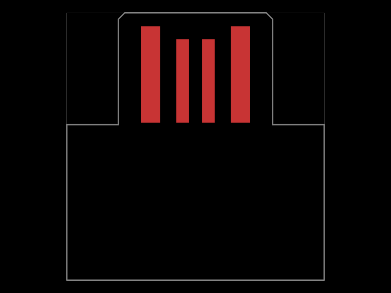 More from this authorpixalynx/edge-connectorConfigures USB-A, Micro-USB, and USB-C PCB-edge connectors with exposed copper contacts and automatically shaped, positioned board tongues.
 Similar packagegokul/usb-hub-boardA 4-layer 100×66 mm USB 2.0 hub board with a USB‑C upstream port, four protected downstream USB‑C/USB‑A ports, an integrated SD card reader, USB hub controllers, 3.3 V regulation, ESD protection, current-limited power switches, crystal oscillators, and filtering/passive components.
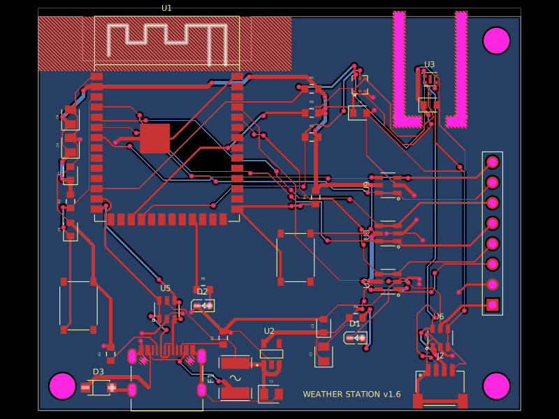 Discover something newolivergrabinski/weather-stationA compact ESP32-S3 Wi‑Fi/Bluetooth module is powered by an AP2112K 3.3 V regulator, with a JST SH connector and blue status LED.