pixalynx/cm5-minimal-carrier
A 4-layer Raspberry Pi CM5 carrier board routes USB‑C 5V power through an RT9742 load switch with TVS protection and capacitive filtering, while providing ESD-protected HDMI output, CM5 connectors, test points, and ground/power planes.
- Version
- 0.1.1
- License
- unset
- Stars
- 0
docs/jlcpcb-order-notes.md
# JLCPCB prototype review notes — revision B

**For quotation and engineering review. Do not treat this file as an approved order.**

## Fabrication parameters

| Item | Requested value |
|---|---|
| Outline | 64 × 60 mm, rectangular |
| Layers | 4; F.Cu / In1.Cu GND / In2.Cu 5 V / B.Cu |
| Stack-up | JLC04161H-3313 specifically; not default 7628 |
| Thickness | Nominal order category 1.6 mm; current calculator label 1.56 mm ±10% finished |
| Copper | 1 oz outer, 0.5 oz inner |
| Finish / mask | ENIG / green |
| Controlled impedance | 100 Ω differential, request ±10% or better and a coupon/report |
| Pair model | L1 non-coplanar, solder mask present, L2 continuous reference |
| Straight pair geometry | Width 0.1234 mm, edge gap 0.2301 mm |
| Smallest track | 0.1234 mm; design floor 0.12 mm |
| Signal copper clearance | Design minimum 0.10 mm |
| Vias | 114 ordinary through-vias, 0.20 mm drill / 0.40 mm land, tent both surfaces |
| Connector stakes | 8 plated routed slots; retain widths and lengths from drill files |
| Nonplated holes | 4 × Ø2.70 mm mounting; 2 × Ø0.65 mm USB pegs |
| Component mask expansion | 0.03 mm per side; probe pads 0.05 mm |
| Minimum nominal mask web | 0.14 mm in current audit; verify final CAM preserves ≥0.10 mm |
| Silkscreen | 1 mm minimum text height, 0.15 mm line/text stroke |
| Common output origin | Board bottom-left `(0,0)`; upper-right `(64,60)` mm |

The 0.5% tolerance shown in the calculator is its numerical search setting. It does **not** replace the requested manufacturing tolerance above. The dielectric and solder-mask assumptions are recorded in `lib/stackup.json`. Any width/spacing/stack-up change must return through the source generator, full build and audit before approval.

## Assembly review

Use `output/jlcpcb-bom.csv`, `output/jlcpcb-cpl-REVIEW.csv` and the top/bottom assembly drawings together. Both CPL sides use the same X/Y coordinate system viewed from above; do not mirror the bottom X coordinates. Rotations are source-footprint rotations, not approved JLC-library corrections. The drawing identifies pad 1/cathode where applicable.

Confirm every placement against the actual JLC component overlay, especially the two 100-pin sockets, USB-C, HDMI, the diode and U1–U4. Connector centroids/rotation registration remain subject to JLC's placement library. C2/C3/C6 require bottom-side assembly. Connector shield stakes need a confirmed mixed SMT/through-hole solder process. All 15 fitted references must be accounted for; TP1–TP6 are bare copper and must not appear in the procurement list.

The exact chosen CM5, cooler, mounting hardware, PSU/cable and enclosure are separate items. The carrier uses a pre-programmed non-wireless eMMC CM5. No blank-module flashing path is provided.

JLC's [assembly FAQ](https://jlcpcb.com/help/article/pcb-assembly-faqs) says it can add fiducials. Confirm its panel/tooling and fiducial arrangement for two-sided assembly; do not add holes or rail features to the finished product outline without reviewing the enclosure.

## Probe map

Coordinates below are in the common fabrication frame, viewed from above. All pads are on **B.Cu** and have no solder paste.

| Pad | Net / purpose | X | Y |
|---|---|---:|---:|
| TP1 | Input VBUS / CM5_5V | 54 | 42 |
| TP2 | GND near input | 52 | 45 |
| TP3 | CM5_5V near module input | 14 | 21 |
| TP4 | GND near module | 14 | 24 |
| TP5 | CM5_3V3 output / GPIO reference | 11 | 27 |
| TP6 | Current-limited HDMI_5V | 46 | 29 |

Measure voltage drop between TP1 and TP3 under load, and probe each rail relative to a nearby ground. TP5 is an output: do not drive it with an external supply. The bare pads are for voltage probing, not current injection or bypassing Type-C negotiation.

## Prototype acceptance additions from MINIMA

Test cold boot, shutdown, USB-C removal/reconnection and recovery with HDMI both connected and disconnected. Repeat with the display on and off, and with independent display/carrier supplies. Record the exact PSU, e-marked 5 A cable, CM5 SKU/firmware and monitor. Check that the rails decay and recover correctly, and investigate any back-power at TP6/TP3 after USB-C removal. A non-e-marked cable comparison must stay within its negotiated 3 A capability and is not a 5 A qualification test.

Also complete the existing inrush, sustained load/temperature, display-mode, ESD and enclosure tests in `fabrication-checklist.md`. This document is prepared locally; it has not been sent to JLCPCB.
Related Packages
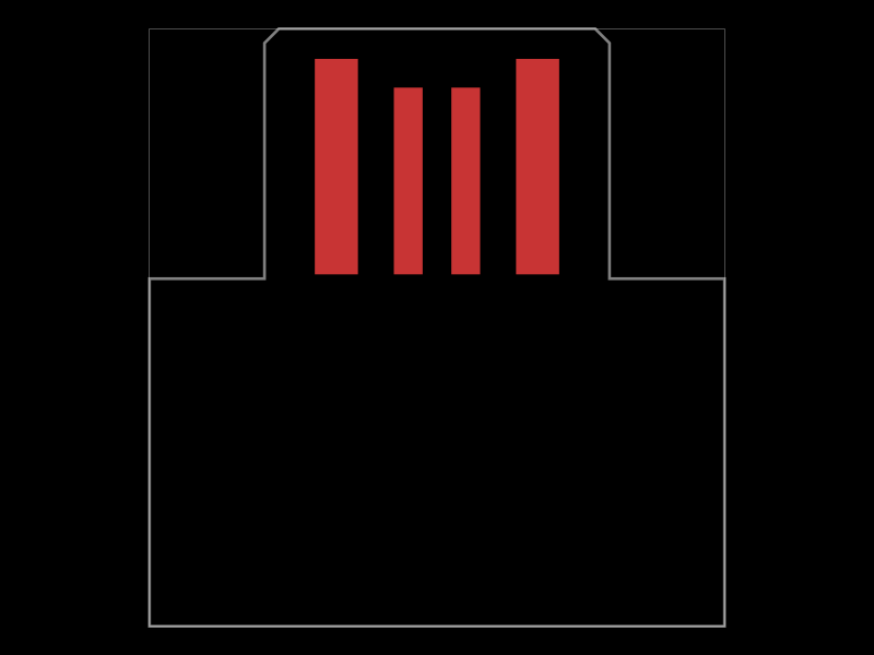 More from this authorpixalynx/edge-connectorConfigures USB-A, Micro-USB, and USB-C PCB-edge connectors with exposed copper contacts and automatically shaped, positioned board tongues.
 Similar packagegokul/usb-hub-boardA 4-layer 100×66 mm USB 2.0 hub board with a USB‑C upstream port, four protected downstream USB‑C/USB‑A ports, an integrated SD card reader, USB hub controllers, 3.3 V regulation, ESD protection, current-limited power switches, crystal oscillators, and filtering/passive components.
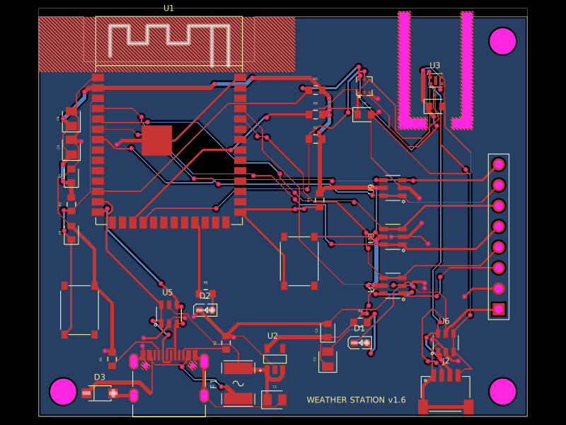 Discover something newolivergrabinski/weather-stationA compact ESP32-S3 Wi‑Fi/Bluetooth module is powered by an AP2112K 3.3 V regulator, with a JST SH connector and blue status LED.