muse/book-reading-clip-lamp
A Wi‑Fi/USB‑C ESP32‑S3 reading lamp with OV5640 camera, microphone, speaker amplifier, rechargeable Li‑Po power management, six-LED boost light, USB protection/charging detection, and a clip/gooseneck enclosure with external FlexPIFA antenna.
- Version
- 0.4.3
- License
- unset
- Stars
- 0
usb-power-policy.txt
Lamp Clip — automatic USB charger detection, 2026-10-12

BEHAVIOR
Recognized BC1.2 DCP/CDP or BQ24392-recognized charging adapter: BQ24074 USB500.
USB-C 1.5 A / 3 A advertisement: BQ24074 USB500 (we do not consume the full advertised current).
Unknown adapter, open data wires, or default-current USB-C with no BC1.2 signature: USB100 until a USB host authorizes 500 mA.
Ordinary SDP computer port: USB100 before enumeration; USB500 only after the host accepts a 500 mA configuration.
No USB-PD negotiation: use 5 V USB power only. The detection circuitry is not an overvoltage protection circuit.

CIRCUIT
U14 BQ24392RSER sits between the connector/ESD and ESP32 USB series resistors. R37/R38 provide 2.2-ohm data ballast; R39 is 2.2 ohms in the detector supply ONLY, not in the charger power path. C38/C39 bypass VBUS_BC. The detector initially isolates the MCU's data termination, classifies the source, then closes the data switch for data-capable sources. GOOD_BAT is tied to VBUS_BC because the BQ24074 power path can supply the system from USB independently of cell state. This avoids a 30-45 minute detector dead-battery timer shutting off off-state charging. It is not a battery health signal. SW_OPEN and CHG_AL_N are unused; CHG_DET is the charging-source permission. Firmware still owns host enumeration, suspend and disconnect.

U15 TUSB320LAIRWBR is strapped as a sink (PORT low), GPIO mode (ADDR floating), enabled (EN_N low). Its internal Rd replaces the removed R1/R2; do not fit extra 5.1k CC resistors. R40 must be 887k, 1%, to VBUS_DET. OUT1 is open-drain, pulled up to its own supply by R41. OUT1 is HIGH for unattached/default-current and LOW for 1.5 A or 3 A; U16 inverts it into CC_FAST. OUT2/OUT3/ID are unused.

U18 TLV75533 generates USB_LOGIC_3V3 from VBUS, independently of the switched V3V3 rail. C43/C44 must have at least 1uF EFFECTIVE capacitance at bias and temperature. C40-C42 bypass the logic ICs. U17 SN74LVC1G332 ORs BC_FAST, CC_FAST and GPIO21 USB_500MA into CHG_EN1 (BQ24074 pin6). R42 holds EN1 low when the detector rail is unpowered. U16/U17 require the specified LVC parts: their Ioff support and 5.5 V-tolerant inputs prevent battery-powered GPIO21 or the approximately 5 V BC_FAST signal backfeeding a dead logic rail. BC_FAST must never connect directly to an ESP32 pin. All new ICs have exact JLCSearch copper and supplier CAD.

BQ24074 pin5 EN2 remains GPIO3 USB_SUSPEND with R13 pull-down. R5 still programs about 500 mA maximum battery current; detected adapters select the 500 mA input mode, not the approximately 957 mA ILIM mode. Lamp/system load, DPPM, temperature, charge taper and tolerances reduce battery current. The USB-powered detectors draw additional current outside the BQ input limit; measure total port current including inrush before claiming USB compliance.

FIRMWARE CONTRACT (not implemented by this PCB)
GPIO21 low on reset/unconfigured host/disconnect; high only after a USB host accepts 500 mA. It need not be raised for a recognized standalone charger. To suspend a USB host, raise GPIO21 FIRST, then GPIO3: EN2/EN1=11. On resume lower GPIO3 FIRST, then apply the host permission policy. Avoid EN2/EN1=10 because it selects ILIM. Preserve these levels during MCU sleep. Hardware detector permission does not remove host suspend obligations. Reset or turning the base off drops MCU controls; suspend across those transitions remains a system-level qualification item. USB100 is not USB suspend.

CHARGE-ONLY MODE
Base SW3 grounds J3.8 through its remote contact to J3.2 to disable TPS63021 V3V3. USB detection and charging stay active. Open J3.8 defaults ON through R25; R36/C37 filter SYS_EN. This disables the large MCU/camera load so a depleted cell can recover without brownout cycling. It is not complete battery isolation. SYS-powered audio/light are held disabled by pull-downs; the SYS-powered orange charge LED remains active. Protected 1S Li-ion/LiPo and a cell-mounted 10k Semitec 103AT-2 NTC remain required.

BENCH ACCEPTANCE BEFORE FABRICATION RELEASE
1. Use a protected cell/battery emulator and correct NTC. Log VBUS, SYS, USB_LOGIC_3V3, EN1/EN2, total USB current and battery current.
2. USB-A BC1.2 DCP: start at USB100; after detection EN1=1/EN2=0 and input transitions to USB500. Repeat with battery depleted, full, disconnected and SW3 OFF/ON. Run a complete off-state charge longer than the old detector dead-battery interval.
3. CDP: verify 500 mA mode and USB enumeration through U14. SDP: remain at 100 mA until authorized; then 500 mA. Verify suspend and resume sequencing and total suspend current.
4. USB-C: test both plug orientations and sources advertising default, 1.5 A, 3 A. OUT1 low only for the latter two. Default-current sources without another authorization stay USB100. Test a slow attach and charge-only cable (no data) fallback.
5. Unplug/replug, MCU reset, off/on while suspended: check EN1/EN2 transitions, no ILIM excursion, no V3V3 backfeed, enumeration reliability and transient port current. Replace the separately flagged Q1 VBUS threshold/discharge circuit before claiming USB attach/detach compliance; it is unchanged here.
6. Check thermal regulation with LEDs/Wi-Fi/audio active and worst-case low cell voltage. Validate the cell's allowed current, TS temperature thresholds and the safety timer. Confirm >1uF effective LDO capacitors and data-line waveform quality including the added switch/ballast.

PRIMARY SOURCES
https://www.ti.com/lit/ds/symlink/bq24392.pdf (pin functions, Table1 charger detection, application ballast/decoupling)
https://www.ti.com/lit/ds/symlink/tusb320lai.pdf (GPIO sink configuration, Table3 OUT1/OUT2, internal Rd, 887k VBUS_DET)
https://www.ti.com/lit/ds/symlink/sn74lvc1g14.pdf (DBV pinout, Schmitt input, Ioff)
https://www.ti.com/lit/ds/symlink/sn74lvc1g332.pdf (DBV pinout, OR truth table, input tolerance, Ioff)
https://www.ti.com/lit/ds/symlink/tlv755p.pdf (DBV pinout and minimum effective input/output capacitance)
https://www.ti.com/lit/ds/symlink/bq24074.pdf (EN2/EN1 table and input/battery current limits)
Related Packages
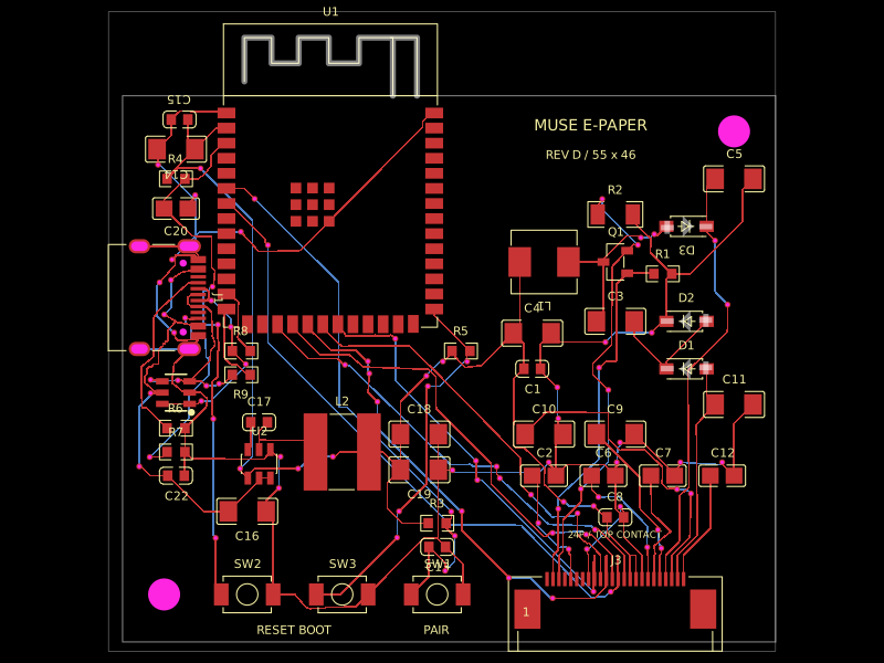 More from this authormuse/esp32-eink-displayA 55×46 mm two-layer ESP32-S3 e-paper controller board with USB‑C power/programming, buck regulation, FPC display connector, UC8179-style boost/charge-pump circuitry, ESD protection, controls, and routed passive components.
 Similar packagepixalynx/usb3-hub-10gA USB 3.2 Gen 2 six-port hub board with USB-C PD power input, regulated 5 V/3.3 V/1.15 V rails, one upstream and four protected downstream USB-A/USB-C ports, SuperSpeed muxes, ESD protection, and controlled port power.
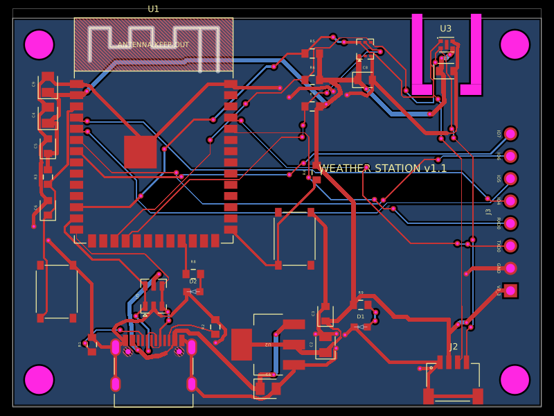 Discover something newolivergrabinski/tscircuit-weatherA 60×44 mm ESP32-S3 Wi‑Fi/BLE weather-station PCB with USB‑C power, 3.3 V regulation and ESD protection, temperature/humidity and UV/light sensors, status LEDs, buttons, Qwiic I²C expansion, debug GPIO header, and a printable enclosure.