muse/book-reading-clip-lamp
A Wi‑Fi/USB‑C ESP32‑S3 reading lamp with OV5640 camera, microphone, speaker amplifier, rechargeable Li‑Po power management, six-LED boost light, USB protection/charging detection, and a clip/gooseneck enclosure with external FlexPIFA antenna.
- Version
- 0.4.3
- License
- unset
- Stars
- 0
imports/B8B_XH_A_LF__SN_.tsx
import type { ChipProps } from "@tscircuit/props"

const pinLabels = {
  pin1: ["pin1"],
  pin2: ["pin2"],
  pin3: ["pin3"],
  pin4: ["pin4"],
  pin5: ["pin5"],
  pin6: ["pin6"],
  pin7: ["pin7"],
  pin8: ["pin8"]
} as const

export const B8B_XH_A_LF__SN_ = (props: ChipProps<typeof pinLabels>) => {
  return (
    <chip
      pinLabels={pinLabels}
      supplierPartNumbers={{
  "jlcpcb": [
    "C157972"
  ]
}}
      manufacturerPartNumber="B8B-XH-A(LF)(SN)"
      // Imported pin 1 was a zero-length pill (equal width/height). The explicit
      // circular hole retains its exact drill/square copper dimensions and avoids
      // core 0.0.1971 assigning a null plated-hole ID to pill + rectPad.
      // Explicit centered offsets also keep the newer connectivity checker from
      // constructing a non-finite drill polygon from undefined offset fields.
      footprint={<footprint>
        <platedhole  portHints={["pin1"]} pcbX="8.750046mm" pcbY="0mm" holeDiameter="0.9000236mm" holeOffsetX={0} holeOffsetY={0} rectPadWidth="1.6999966mm" rectPadHeight="1.6999966mm" pcbRotation="180deg" shape="circular_hole_with_rect_pad" />
<platedhole  portHints={["pin2"]} pcbX="6.249924mm" pcbY="0mm" outerDiameter="1.6999966mm" holeDiameter="0.9000236mm" shape="circle" />
<platedhole  portHints={["pin3"]} pcbX="3.750056mm" pcbY="0mm" outerDiameter="1.6999966mm" holeDiameter="0.9000236mm" shape="circle" />
<platedhole  portHints={["pin4"]} pcbX="1.249934mm" pcbY="0mm" outerDiameter="1.6999966mm" holeDiameter="0.9000236mm" shape="circle" />
<platedhole  portHints={["pin5"]} pcbX="-1.249934mm" pcbY="0mm" outerDiameter="1.6999966mm" holeDiameter="0.9000236mm" shape="circle" />
<platedhole  portHints={["pin6"]} pcbX="-3.750056mm" pcbY="0mm" outerDiameter="1.6999966mm" holeDiameter="0.9000236mm" shape="circle" />
<platedhole  portHints={["pin7"]} pcbX="-6.249924mm" pcbY="0mm" outerDiameter="1.6999966mm" holeDiameter="0.9000236mm" shape="circle" />
<platedhole  portHints={["pin8"]} pcbX="-8.750046mm" pcbY="0mm" outerDiameter="1.6999966mm" holeDiameter="0.9000236mm" shape="circle" />
<silkscreenpath route={[{"x":-11.219967399999973,"y":-0.9163812000000462},{"x":-10.599978799999917,"y":-0.9163812000000462},{"x":-10.599978799999917,"y":2.7999944000000596},{"x":10.59997880000003,"y":2.7999944000000596},{"x":10.59997880000003,"y":-0.7999984000000495},{"x":10.59997880000003,"y":-0.8999981999999136},{"x":11.219967399999973,"y":-0.8999981999999136}]} />
<silkscreenpath route={[{"x":-7.951622399999906,"y":-2.3500080000000025},{"x":-7.951622399999906,"y":-1.7779999999999063},{"x":7.874000000000137,"y":-1.7779999999999063},{"x":7.999984000000154,"y":-1.7779999999999063},{"x":7.999984000000154,"y":-2.3500080000000025}]} />
<silkscreenpath route={[{"x":11.154867200000012,"y":-1.749298000000067},{"x":9.078899800000158,"y":-1.749298000000067},{"x":9.078899800000158,"y":-2.3499825999999757}]} />
<silkscreenpath route={[{"x":-11.219967399999973,"y":-1.7493233999999802},{"x":-9.143999999999892,"y":-1.7493233999999802},{"x":-9.143999999999892,"y":-2.3500080000000025}]} />
<silkscreenpath route={[{"x":-11.219967399999973,"y":-2.3500080000000025},{"x":11.219967399999973,"y":-2.3500080000000025}]} />
<silkscreenpath route={[{"x":11.219967399999973,"y":-2.3500080000000025},{"x":11.219967399999973,"y":3.399967800000013}]} />
<silkscreenpath route={[{"x":11.219967399999973,"y":3.399967800000013},{"x":-11.219967399999973,"y":3.399967800000013}]} />
<silkscreenpath route={[{"x":-11.219967399999973,"y":3.39999320000004},{"x":-11.219967399999973,"y":-2.3500080000000025}]} />
<silkscreentext text="{NAME}" pcbX="0mm" pcbY="4.429mm" anchorAlignment="center" fontSize="1mm" />
<fabricationnotepath route={[{"x":-11.100003199999946,"y":-1.8999961999999186},{"x":-9.300006799999892,"y":-1.8999961999999186},{"x":-9.300006799999892,"y":-2.2999953999999434},{"x":-11.100003199999946,"y":-2.2999953999999434},{"x":-11.100003199999946,"y":-1.8999961999999186}]} strokeWidth="0.254mm" />
<fabricationnotepath route={[{"x":-7.7999843999998575,"y":-1.8999961999999186},{"x":7.899984200000063,"y":-1.8999961999999186},{"x":7.899984200000063,"y":-2.2999953999999434},{"x":-7.7999843999998575,"y":-2.2999953999999434},{"x":-7.7999843999998575,"y":-1.8999961999999186}]} strokeWidth="0.254mm" />
<fabricationnotepath route={[{"x":9.288322800000174,"y":-1.847113400000012},{"x":11.0883192,"y":-1.847113400000012},{"x":11.0883192,"y":-2.2471126000000368},{"x":9.288322800000174,"y":-2.2471126000000368},{"x":9.288322800000174,"y":-1.847113400000012}]} strokeWidth="0.254mm" />
<fabricationnotepath route={[{"x":-11.09997779999992,"y":-0.7999984000000495},{"x":-10.699978599999895,"y":-0.7999984000000495},{"x":-10.699978599999895,"y":2.899994200000151},{"x":10.799978400000214,"y":2.899994200000151},{"x":10.799978400000214,"y":-0.7999984000000495},{"x":11.09997779999992,"y":-0.7999984000000495},{"x":11.09997779999992,"y":3.2999933999999485},{"x":-11.09997779999992,"y":3.2999933999999485},{"x":-11.09997779999992,"y":-0.7999984000000495}]} strokeWidth="0.254mm" />
<courtyardoutline outline={[{"x":-11.499964800000043,"y":3.5499933999999485},{"x":11.49999020000007,"y":3.5499933999999485},{"x":11.49999020000007,"y":-2.649995200000035},{"x":-11.499964800000043,"y":-2.649995200000035},{"x":-11.499964800000043,"y":3.5499933999999485}]} />
      </footprint>}
      cadModel={{
        objUrl: "https://modelcdn.tscircuit.com/easyeda_models/assets/C157972.obj?uuid=54a71534409e4820936ccd38b1b08831",
        stepUrl: "https://modelcdn.tscircuit.com/easyeda_models/assets/C157972.step?uuid=54a71534409e4820936ccd38b1b08831",
        pcbRotationOffset: 180,
        modelOriginPosition: { x: 8.750012699999957, y: 2.700499100000014, z: -1.800005 },
      }}
      {...props}
    />
  )
}
Related Packages
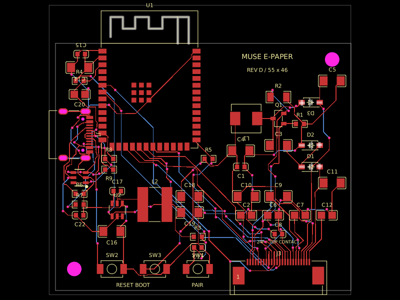 More from this authormuse/esp32-eink-displayA 55×46 mm two-layer ESP32-S3 e-paper controller board with USB‑C power/programming, buck regulation, FPC display connector, UC8179-style boost/charge-pump circuitry, ESD protection, controls, and routed passive components.
 Similar packagepixalynx/usb3-hub-10gA USB 3.2 Gen 2 six-port hub board with USB-C PD power input, regulated 5 V/3.3 V/1.15 V rails, one upstream and four protected downstream USB-A/USB-C ports, SuperSpeed muxes, ESD protection, and controlled port power.
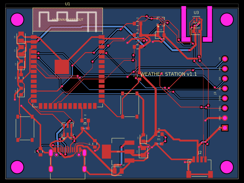 Discover something newolivergrabinski/tscircuit-weatherA 60×44 mm ESP32-S3 Wi‑Fi/BLE weather-station PCB with USB‑C power, 3.3 V regulation and ESD protection, temperature/humidity and UV/light sensors, status LEDs, buttons, Qwiic I²C expansion, debug GPIO header, and a printable enclosure.