muse/book-reading-clip-lamp
A Wi‑Fi/USB‑C ESP32‑S3 reading lamp with OV5640 camera, microphone, speaker amplifier, rechargeable Li‑Po power management, six-LED boost light, USB protection/charging detection, and a clip/gooseneck enclosure with external FlexPIFA antenna.
- Version
- 0.4.3
- License
- unset
- Stars
- 0
component-provenance.csv
Reference,Manufacturer part number,JLC part,Imported source,Footprint handling,Electrical mapping
U1,ESP32-S3-WROOM-1U-N16R8,C3013946,imports/ESP32_S3_WROOM_1U_N16R8.tsx,JLC land pattern; pad 26 coordinate corrected; masked links join exposed ground lands,Espressif datasheet mapping overrides incorrect catalog names; PSRAM pins28-30 unused
U2,BQ24074RGTR,C54313,imports/BQ24074RGTR.tsx,Exact JLCSearch/EasyEDA footprint,TI physical pins 1-17; ground and input metadata supplied
U3,TPS63021DSJR,C202140,imports/TPS63021DSJR.tsx,Exact JLCSearch/EasyEDA footprint including comb thermal land; placed at 270 degrees,TI physical pins 1-15; pin 13 PS_SYNC restored
U4,INMP441ACEZ-R7,C22379536,imports/INMP441ACEZ_R7.tsx,JLC polygon lands preserved; added 0.5 mm acoustic hole and masked ground escape; polygon origins normalized,TDK physical pins 1-9; pin 4 L/R restored
U5,MAX98357AETE+T,C910544,imports/MAX98357AETE_T.tsx,Exact JLCSearch/EasyEDA footprint,ADI physical pins 1-17 overridden with verified names
U6,TPS61165DBVR,C58756,imports/TPS61165DBVR.tsx,Exact JLCSearch/EasyEDA footprint,TI physical pins 1-6
U7,USBLC6-2SC6,C7519,imports/USBLC6_2SC6.tsx,Exact JLCSearch/EasyEDA footprint,ST pin1/6=I/O1 and pin3/4=I/O2
Q1,"2N7002,215",C65189,imports/A_2N7002_215.tsx,Exact JLCSearch/EasyEDA footprint,Nexperia pin1=gate pin2=source pin3=drain
D1,MBR0540T1G,C21353,imports/MBR0540T1G.tsx,Exact JLCSearch/EasyEDA footprint,ONsemi pin1=cathode pin2=anode
LED1-LED6,XL-3216WWC,C965830,imports/XL_3216WWC.tsx,JLC component with manufacturer recommended LED copper land override,Pin1=cathode pin2=anode
J2,FH12-24S-0.5SH(55),C202112,imports/FH12_24S_0_5SH_55_.tsx,Exact JLCSearch land pattern and CAD model,Seeed114993115 MJY5OAF-F3M-V1 drawing2023-06-20 p3; pin11 DOVDD1.8 V; pin23 AF ground; pin10 internal DVDD;24 contacts plus2 hold-downs
U8,TLV75528PDBVR,C2868951,imports/TLV75528PDBVR.tsx,Exact JLCSearch land pattern and CAD model,TI DBV pins1IN2GND3EN4NC5OUT
U9,TLV75518PDBVR,C2877863,imports/TLV75518PDBVR.tsx,Exact JLCSearch land pattern and CAD model,TI DBV pins1IN2GND3EN4NC5OUT
U10; U11,SN74AXC8T245PWR,C882718,imports/SN74AXC8T245PWR.tsx,Exact JLCSearch land pattern and CAD model,TI PW24 A3.3 V B1.8 V; both DIR pins LOW select all B-to-A; OE CAM_PWDN3.3 V
U12,SN74LVC125APWR,C7813,imports/SN74LVC125APWR.tsx,Exact JLCSearch land pattern and CAD model,TI PW14;1.8 V outputs;3.3 V tolerant inputs
U13,TXS0102DCTR,C324082,imports/TXS0102DCTR.tsx,Exact JLCSearch land pattern and CAD model,TI DCT8;A1.8 V B3.3 V; OE1.8 V RESET
LED7,XL-1608SYGC-06,C965805,imports/XL_1608SYGC_06.tsx,JLC exact copper and CAD; board rotation180 degrees,pin1 cathode; pin2 anode
LED8,XL-1608UOC-06,C965800,imports/XL_1608UOC_06.tsx,JLC copper sizes and CAD retained; catalog pad numbering corrected to match manufacturer cathode mark and silk/fab; board rotation180 degrees,Manufacturer page7 pin1 cathode; pin2 anode
SW1,PV5S24011G,,base-assembly-geometry.ts,Off-board panel part; no copper footprint; dimensional reference,Official E-Switch PV5 family dimensions; gold solder-lug variant
SW3,100SP1T1B1M1REH,,base-assembly-geometry.ts,Off-board panel part; no copper footprint; dimensional reference,Official E-Switch 100-series SP1 T1 B1 M1 R drawings
J3,B8B-XH-A(LF)(SN),C157972,imports/B8B_XH_A_LF__SN_.tsx,Exact imported dimensions and supplier CAD; 2.50 mm pitch / 0.90 mm drills; pin1 equivalent circular-hole square-pad representation avoids core null ID,1 VBAT; 2 GND; 3 NTC; 4 GND; 5 SPK_P; 6 SPK_N; 7 ASK_REMOTE; 8 PWR_REMOTE
U14,BQ24392RSER,C128408,imports/BQ24392RSER.tsx,Exact JLCSearch footprint and supplier CAD; TI pinout verified,Pins 7/8 connector data; 3/2 MCU data; CHG_DET is 5V-domain and only feeds tolerant logic.
U15,TUSB320LAIRWBR,C132554,imports/TUSB320LAIRWBR.tsx,Exact JLCSearch footprint and supplier CAD; TI pinout verified,GPIO sink mode; internal CC Rd replaces R1/R2; OUT1 low for 1.5A/3A advertisements.
U16,SN74LVC1G14DBVR,C7835,imports/SN74LVC1G14DBVR.tsx,Exact JLCSearch footprint and supplier CAD; TI pinout verified,Pin2 input; pin4 output; pin3 GND; pin5 USB_LOGIC_3V3; pin1 NC.
U17,SN74LVC1G332DBVR,C43368,imports/SN74LVC1G332DBVR.tsx,Exact JLCSearch footprint and supplier CAD; TI pinout verified,Pin1 BC_FAST; pin3 CC_FAST; pin6 USB_500MA; pin4 CHG_EN1; pin2 GND; pin5 USB_LOGIC_3V3. 5.5V-tolerant inputs and Ioff required.
U18,TLV75533PDBVR,C404027,imports/TLV75533PDBVR.tsx,Exact JLCSearch footprint and supplier CAD; TI pinout verified,VBUS supplies IN/EN; works with the base switch OFF; separate from switched V3V3.
Related Packages
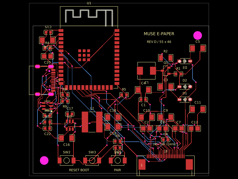 More from this authormuse/esp32-eink-displayA 55×46 mm two-layer ESP32-S3 e-paper controller board with USB‑C power/programming, buck regulation, FPC display connector, UC8179-style boost/charge-pump circuitry, ESD protection, controls, and routed passive components.
 Similar packagepixalynx/usb3-hub-10gA USB 3.2 Gen 2 six-port hub board with USB-C PD power input, regulated 5 V/3.3 V/1.15 V rails, one upstream and four protected downstream USB-A/USB-C ports, SuperSpeed muxes, ESD protection, and controlled port power.
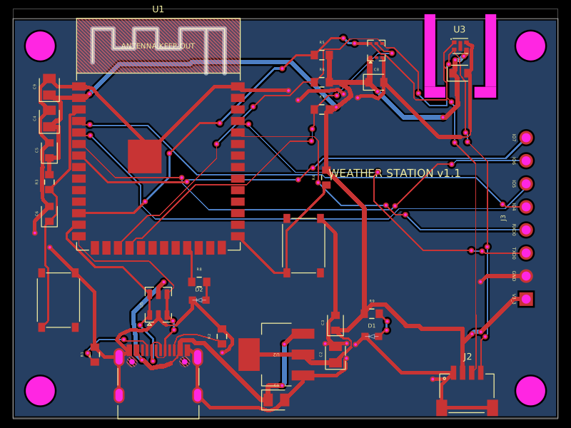 Discover something newolivergrabinski/tscircuit-weatherA 60×44 mm ESP32-S3 Wi‑Fi/BLE weather-station PCB with USB‑C power, 3.3 V regulation and ESD protection, temperature/humidity and UV/light sensors, status LEDs, buttons, Qwiic I²C expansion, debug GPIO header, and a printable enclosure.