muse/book-reading-clip-lamp
A Wi‑Fi/USB‑C ESP32‑S3 reading lamp with OV5640 camera, microphone, speaker amplifier, rechargeable Li‑Po power management, six-LED boost light, USB protection/charging detection, and a clip/gooseneck enclosure with external FlexPIFA antenna.
- Version
- 0.4.3
- License
- unset
- Stars
- 0
camera-sourcing.txt
LAMP CLIP - SEEED CAMERA SOURCING AND CONNECTION (0.3.0)
06 October 2026 | Engineering design; no physical camera sample tested

CAMERA TO ORDER
Seeed Studio SKU 114993115: OV5640 Camera for XIAO ESP32S3 Sense (With Heat Sink)
https://www.seeedstudio.com/OV5640-Camera-for-XIAO-ESP32S3-Sense-With-Heat-Sink-p-5739.html
Alternative US retailer:
https://www.digikey.com/en/products/detail/seeed-technology-co-ltd/114993115/21277047
Module drawing MJY5OAF-F3M-V1 dated 2023-06-20, PDF page 3:
https://files.seeedstudio.com/wiki/OV5640_for_ESP32S3_sense/OV5640_Datasheet.pdf
Autofocus examples:
https://wiki.seeedstudio.com/xiao_esp32s3_camera_usage/

This is a sensor/lens assembly on its flex ribbon plus heat sink. The custom
lamp PCB contains the regulators and level conversion. No XIAO motherboard
or breakout board is needed. Order the exact SKU and inspect the shipped
revision. No price, stock, delivery time or close-focus guarantee is embedded
in the design. No purchase has been placed by this task.

ELECTRICAL INTERFACE
OV5640, 5 MP, 8-bit parallel DVP, SCCB control, autofocus.
U1 remains ESP32-S3-WROOM-1U-N16R8, 16 MB flash / 8 MB PSRAM.
https://github.com/espressif/esp32-camera
Pin 11 DOVDD=1.8 V from U9 TLV75518. Pin 4 AVDD and pin 24 AFVDD=2.8 V
from U8 TLV75528. Pin 23=AF-GND. Pin 10 is the module's internal 1.5 V
core rail, decoupled by C24 2.2 uF and C25 100 nF, with no external driver.
OmniVision prefers internal DVDD when DOVDD is 1.8 V (sensor datasheet 2.7).
Do not enable an external-core configuration or bridge pin 10 to a supply.
See camera-pinout.csv; another OV5640 camera is not automatically compatible.
The former KLT camera used pin 11=2.8 V and pin 23=NC; do not fit it here.

U10/U11 SN74AXC8T245: A side VCCA=3.3 V MCU, B side VCCB=1.8 V camera.
DIR1=DIR2=LOW -> all B-to-A channels (TI table 7-1). OE=CAM_PWDN, referenced
to 3.3 V, disables image outputs at reset. Unused U11 camera inputs are
held LOW and their MCU outputs are unconnected. Both supplies are bypassed.
U12 SN74LVC125 powered at 1.8 V safely accepts 3.3 V MCU clock/reset/powerdown.
R33 is 33 ohm XCLK series termination. U13 TXS0102 has A=1.8 V, B=3.3 V;
its internal SCCB pull-ups are retained and OE follows 1.8 V FPC_RESET.
No direct 3.3 V output may be connected to the flex.

CONNECTOR AND MECHANICS
J2 Hirose FH12-24S-0.5SH(55), JLC C202112, bottom contacts, 24 x 0.5 mm.
https://www.hirose.com/product/p/CL0586-0521-0-55
Seeed drawing: tail 12.5 mm wide, 0.5 mm pitch, 0.3 +/-0.03 mm thickness,
2.5 mm contact length; assembly length 70.5 mm. Camera body 8.5 x 8.5 mm;
module drawing total height about 5.4 mm before any added heat-sink clearance.
The current J2 is NOT a documented mechanical match: Seeed has 2.5 mm contacts
and a 4 mm stiffener; Hirose recommends 3.5 mm and 4.5 mm minimum respectively.
Select/qualify a short-tail connector before PCB fabrication; the old claim of
a mechanical match is withdrawn. See mechanical/camera-fit-notes.txt.
The drawing's bottom view shows the contact side; inspect contact beams and
pin 1, not only the appearance of a mirrored PCB preview. Pads 25/26 are
mechanical hold-downs, not camera contacts, and connect to GND.

J2 is internal on the page-facing bottom side, with inward ribbon insertion.
Allow latch access, nonconductive lens retention and a gentle storage fold for
the longer flex. Do not crease at the lens bond. The 9 mm silkscreen box is
only an alignment guide. Check the supplied heat sink's final envelope before
freezing the head enclosure. M5 models the body, the supplied 7 x 6 x 7 mm heatsink and a 62 mm edge-to-tip
folded ribbon; see mechanical/camera-fit-notes.txt. Fin/barrel detail is approximate.
The shell is 28 mm deep; the old 22 mm shell does not fit the supplied heatsink.
Insert/remove with all power disconnected, close the latch evenly and retain
the lens separately so the flex carries no mechanical load.

BRING-UP AND LIMITS
U9 starts DOVDD; R34/C32 (10k/1uF) delays the U8 enable to bring up AVDD/AF
later. This nominal RC delay is not a precision power-good supervisor: scope
DOVDD stable before AVDD stable with actual capacitor tolerance, loads and
power sources. Internal core voltage is generated by the camera after mating.
CAM_PWDN defaults HIGH; CAM_RESET and CAM_XCLK default LOW.
After rails are stable, wait at least 5 ms, start XCLK, release PWDN and RESET
with at least 1 ms clock/reset timing, then wait 20 ms before SCCB initialization
(sensor datasheet 2.7.1/2.8). Perform the required >=1 ms hardware reset pulse.
Load autofocus firmware and wait for focusing before capturing a JPEG into PSRAM.
Start with 10 MHz XCLK and one frame buffer; qualify higher clock rates against
translator propagation, ribbon loading and actual clock/data timing. Test
focus at the actual page distance, image orientation, lighting/PWM and page
legibility; no optical or timing qualification is claimed by the circuit checks.
Sensor sequencing source:
https://files.seeedstudio.com/wiki/SeeedStudio-XIAO-ESP32S3/res/OV5640_datasheet.pdf
Translator sources:
https://www.ti.com/lit/ds/symlink/sn74axc8t245.pdf
https://www.ti.com/lit/ds/symlink/sn74lvc125a.pdf
https://www.ti.com/lit/ds/symlink/txs0102.pdf
Related Packages
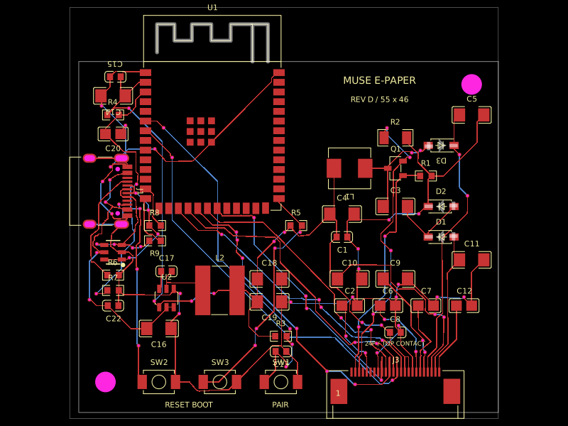 More from this authormuse/esp32-eink-displayA 55×46 mm two-layer ESP32-S3 e-paper controller board with USB‑C power/programming, buck regulation, FPC display connector, UC8179-style boost/charge-pump circuitry, ESD protection, controls, and routed passive components.
 Similar packagepixalynx/usb3-hub-10gA USB 3.2 Gen 2 six-port hub board with USB-C PD power input, regulated 5 V/3.3 V/1.15 V rails, one upstream and four protected downstream USB-A/USB-C ports, SuperSpeed muxes, ESD protection, and controlled port power.
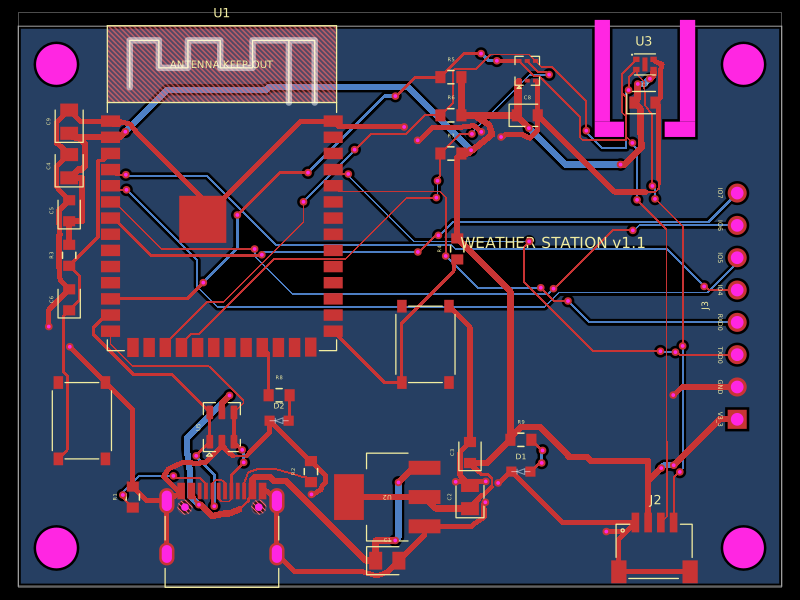 Discover something newolivergrabinski/tscircuit-weatherA 60×44 mm ESP32-S3 Wi‑Fi/BLE weather-station PCB with USB‑C power, 3.3 V regulation and ESD protection, temperature/humidity and UV/light sensors, status LEDs, buttons, Qwiic I²C expansion, debug GPIO header, and a printable enclosure.