mohan-bee/stm32-midi-keys
Clips rectangular ground-region geometry to fit within the board’s scaled rounded-edge outline using polygon intersection.
- Version
- 1.0.2
- License
- unset
- Stars
- 0
ISSUES.md
PCB

Schematic

# High-priority issues encountered

Tested 2026-10-08 with `tscircuit 0.0.2769`, `@tscircuit/core 0.0.2110`,
`@tscircuit/cli 0.1.2265`, `kicad-to-circuit-json 0.0.142`, and `kicadts 0.0.53`.
These are local findings, not submitted upstream issues. Source-board findings
are separated below. Reproduction commands run from this directory.

Update 2026-10-09: JLCPCB integration was tested with `tscircuit 0.0.2783`,
`@tscircuit/core 0.0.2114`, `@tscircuit/cli 0.1.2271`, and
`@tscircuit/capacity-autorouter 0.0.963`. The four-phase fixed-route fallback
failure also reproduces on 0.0.963. Pipeline 7 instead exhausted its iterations
in the digital/control phase on 0.0.958. See the current README for the final
routing configuration; historical repro descriptions below retain their versions.

## Current native autoroute — remaining high-priority findings

The final two-phase run completes with 169 traces / 240 vias and preserves all
14 touch-electrode nets. It is **not fabrication-ready**. Native DRC still reports:

- Via drill overlaps with U1 pad 4 at (-31.89, 23.17), C11 pad 1 at
  (-38.77, 23.11), and R3 pad 2 at (3.19, 19.85) mm. These need routing repair;
  completed solver phases are not evidence that drill/pad clearance passed.
- OSC_IN and OSC_OUT have 4 and 2 vias respectively, despite the crystal
  primitive's zero-via constraint. The phase's Simple Route JSON does not carry
  those source-trace via limits, and final DRC detects the violations afterward.

There is also a 339.40 mm total GND-route length versus the explicit 300 mm
whole-net limit. That override addresses the decoupling-rule problem below;
it does not validate individual decoupling connections. No unconnected-port
errors are reported in the final output. Exact records are retained in
`autorouted.circuit.json`, with counts in `validation/summary.json`.

**Additional keepout limitation:** KEY_AS reaches y=4.65048 mm, below the intended
electronics strip boundary y=10.8 mm. The original track/via-only key-area rule
is not preserved. Inspection of core shows `autoroutingphase.region` only defines
a regional problem when `reroute` is enabled; it is not a general routing fence.
The previously supplied ordinary-phase region props were therefore ineffective
and have been removed. Unbroken top-side electrode pours prevent those electrodes
from being cut by top tracks, but do not prohibit bottom tracks beneath the keys.
This is additional evidence that the native keepout workaround is incomplete.

## P1 — Omitted hole offsets can crash copper cleanup after routing succeeds

**Reproduce here:** In `top-access-footprint.tsx`, omit `holeOffsetX` and
`holeOffsetY` from the `circular_hole_with_rect_pad` primitives, then build.
These are optional primitive props. Both routing phases finish (169 traces),
but copper cleanup throws `undefined is not an object (evaluating
'node.item.key.low')` from `@flatten-js/core`, called by `copperPolygonsTouch`.

**Cause observed:** `getPlatedHolePolygon` adds `pad.hole_offset_x/y` to the pad
coordinates without defaulting missing offsets to zero. The resulting drill
circle has NaN coordinates. `validation/copper-cleanup-failure.log` preserves
the stack; `validation/copper-cleanup-failing-polygons.json` records the malformed
circle (NaN serializes as null).

**Impact:** A completed autoroute cannot be saved as final Circuit JSON. The CLI
also leaves an older output file behind, so file existence is not proof of a
successful current build.

**Workaround here:** Explicitly set both hole offsets to zero. No dependency
source patches are required or retained. The geometry utility should supply
zero defaults and reject non-finite geometry before calling the distance tree.

## P1 — Automatic decoupling length is applied to an entire shared supply net

**Reproduce:** Instantiate the imported STM32 with its power-pin attributes,
100 nF capacitors, and the board's multi-terminal GND / supply `<trace path>`
declarations. Omit the explicit `maxDecouplingTraceLength` overrides.

**Actual:** Native capacitors receive `max_decoupling_trace_length: 1`. This
propagates to `max_length: 1` on the entire GND, P3V3, P5V, and analog-supply
source traces. Routing is refused because endpoints on opposite sides of the
170 mm board cannot be within 1 mm. One error names U3.pin2 to J1.pin1 and
reports endpoints 155.41 mm apart.

**Impact:** Adding real imported part attributes makes the previously routable
netlist fail before the autorouter starts. A local decoupling requirement should
constrain the corresponding IC/capacitor connection, not every terminal on a rail.

**Workaround here:** Explicit 300 mm `maxDecouplingTraceLength` on native
capacitors to allow the preserved whole-board rail declarations to route.
This avoids the incorrect global 1 mm constraint; it does **not** establish
that local decoupling placement or loop inductance is acceptable.

## P1 — JLCPCB crystal import omits required load capacitance

**Reproduce:** `bunx tsci import --jlcpcb C400090 --exclude-pin-attributes`.
The generated `TAXM8M4RDBCCT2T` uses `<crystal frequency="8MHz"
pinVariant="four_pin" ...>` without `loadCapacitance`.

**Actual here:** The crystal had no usable ports, and the netlist check reported
three missing Y1 port selectors. The shared GND trace consequently failed to
connect, producing additional floating MCU-ground errors.

**Workaround here:** Add `loadCapacitance="10pF"`, matching the selected part's
catalog value. The netlist check then passes. Import generation should include
this required electrical value or clearly require the caller to provide it.

## P1 — KiCad parser rejects valid offset-only SMD drill metadata and hatch fill settings

**Reproduce:** Add `source/stm32_midi_keys.kicad_pcb` unmodified to
`KicadToCircuitJsonConverter`, then call `runUntilFinished()`.

**Actual:** `drill requires a diameter value` on the 14 touch electrodes.
After removing those fields, parsing fails with
`Class "mode" not registered for parent "fill"` on the hatched bottom ground zone.
KiCad opens and plots the same original file.

**Impact:** The board cannot be imported directly. Crucially, simply removing
`(drill (offset 0 0.95))` changes the copper geometry: TK1's anchor is
(50.925, 58) mm, but KiCad's `PAD.ShapePos(F_Cu)` is (50.925, 58.95) mm.
Dropping the offset puts electrode copper over nearby resistor pads.

**Workaround here:** Normalize unsupported parser fields in memory only; retain
all saved zone-fill polygon coordinates; restore actual pad copper centers from
KiCad's own API using `source/pad-shapes.json`. Also merge JP1's decomposed
custom-pad pieces back into individual copper polygons. Original file is untouched.

**Expected fix:** Parse offset-only drill metadata independently from hole diameter,
apply offsets to SMD copper, and accept KiCad hatch settings without deleting them.

## P1 — Whole-board Circuit JSON inflation silently loses essential PCB content

**Reproduce:** `bunx tsci build repros/inflation.circuit.tsx --disable-parts-engine`.
Its default export returns `<board circuitJson={circuitJson} schematicDisabled routingDisabled />`.

**Observed on the initial conversion:** 29 copper pours became zero, so every touch
electrode disappeared. The 170 × 60 mm outline became rectangular, thickness
changed from 1.6 to 1.4 mm, and 294 input trace records became 255 output records.
Via records increased from 124 to 223. Record counts alone do not prove every
geometric difference, but losing the entire touch-electrode layer does.

**Impact:** A plausible component-and-track preview no longer represents the
original touch keyboard. `routingDisabled` does not make this a lossless import.

**Workaround here:** Keep a direct native Circuit JSON reference, and build the
autorouted TSX with explicit board dimensions/outline, native components,
native net/trace declarations, native copper pours, and native routing phases.

## P1 — KiCad routing keepouts are silently omitted

**Reproduce:** Run `bun run import:board`; compare `source/geometry.json` with
the imported Circuit JSON. Source has four keepout zones, output has no
`pcb_keepout` records and the converter emits no warnings.

**Impact:** An autorouter can place tracks/vias beneath the capacitive electrodes
or in the edge exclusion region. These constraints matter to touch sensing.

**Workaround here:** An initial native-keepout attempt reproduced the separate
pour-erasure problem below. Final TSX uses reserved (`unbroken`) electrode pours
and restricts routing phases to the electronics strip. Original keepouts remain
in `source/geometry.json` and KiCad. This is not equivalent to the original
both-layer track/via-only exclusion rules, particularly around the octave keys.

**Expected fix:** Preserve keepout polygons, holes, layer coverage, and distinct
track/via/pad/pour permissions; warn for unsupported constraints.

## P1 — Completed phased autorouting produces a PCB that fails electrical DRC

**Reproduce:** `bun run build`. All four phases use the native `auto_local`
autorouter, with no copied KiCad routes as input. Inspect
`dist/autorouter-debug/phase-*.input.simple-route.json` and corresponding outputs.

**Observed first complete run:** Each phase reported `errors=0`; the final output
contained 169 traces, but core checks reported 38 trace errors, four pad/trace
clearance errors, 11 via/trace clearance errors, seven pad/via clearance errors,
and 17 placement errors. Two edge-clearance issues came from source ground
outlines and have a separate local workaround; the cross-net contacts cannot
be explained by those outlines.

Examples from `validation/first-phased-run/circuit.json`:

- `SW2.pin3 to SW2.pin4` overlaps `U3.pin2 to J1.pin1` (accidental contact).
- `R25.pin2 to J3.pin4` overlaps `JP1.pin1 to C7.pin1` (accidental contact).
- A via near C9 has 0.068 mm clearance where 0.1 mm is required.
- Native traces terminating on touch-pad centers enter the electrode keepout.
  KiCad's original routes can terminate at the offset pad anchors instead;
  this endpoint/keepout case needs distinct treatment from cross-net shorts.

The CLI correctly exits nonzero after DRC. The issue is the solver result's
zero-error status and invalid geometry, not a falsely successful CLI exit.
The generated autorouted board is therefore **not fabrication-ready**.

**Expected fix:** Validate cross-phase copper, via/hole clearances, and keepouts
against the same constraints used by final core checks; return failures to the
router repair step instead of treating solver completion as a clean route.

## P1 — Native keepouts cannot preserve track-only restrictions over touch copper

**Reproduce:** Use the original touch outlines as `<copperpour>` elements and
place `<keepout allowPlacements allowTraces={false} layers={['top','bottom']}>`
over the key area. The source KiCad rule prohibits tracks/vias but explicitly
permits pads and copper pours.

**Actual:** The completed native output contains only GND pours; all 14 touch
electrode pours disappear. Inspection of `@tscircuit/copper-pour-solver` shows
`pcb_keepout` records are converted to copper obstacles without an independent
allow-copper-pour rule.

**Impact:** Restoring imported keepouts using the native primitive destroys
essential functional copper. A correct-looking routing obstacle is insufficient.

**Workaround here:** Remove the blanket keepout elements and use `unbroken` touch
electrode pours. This restores electrode generation but does not preserve the
original track/via-only restriction. The earlier phase-region workaround was
ineffective for ordinary routing; see the measured excursion above. A full fix
requires distinct track/via/pad/pour permissions throughout import, routing,
pour generation, and DRC.

## P1 — Final phase regional fallback crashes on a fixed route from an earlier phase

**Reproduce with the final project:** `bun run build`. The first three phases
complete (21, 52, then 100 cumulative traces). The power/ground phase fails with:

```
Pipeline9 could not promote fixed route "source_net_27_fixed_30_2" into the active regional fallback (capacity-autorouter@0.0.958)
```

The CLI renders the same net as `net.OSC_IN_fixed_30_2` in its readable log.
This happened on both an uncached run and a subsequent run using cached earlier
phases. See `validation/regional-failure/` for the input and earlier trace output.

**Impact:** The final native Circuit JSON contains no PCB traces/vias after this
failure, although the earlier phase outputs were successfully saved. There are
67 reported unconnected-port groups in that incomplete final result. The native
output still contains all 86 components and 14 touch-electrode nets.

**Expected fix:** Preserve supported fixed-route geometry when creating regional
fallback inputs. If the final phase cannot finish, expose prior completed phases
as an explicitly incomplete result rather than losing them from the final board.

**Status:** Still reproducible with four phases, including autorouter 0.0.963.
The current board works around it using two phases (USB/clock, then all remaining
nets). Both now finish and the final native Circuit JSON contains their tracks.
The remaining DRC issues are listed at the top of this file.

## Source-board findings — not tscircuit bugs

`validation/kicad-drc.json` comes from KiCad CLI against the untouched source.
It reports two unconnected items: a disconnected top GND zone island and an
OSC_IN connection between U1 pad 5 and a bottom-layer track. It also reports
two copper-edge clearance violations and one zone intersection, plus library
and silkscreen warnings. Source PCB geometry was preserved in the reference;
those original findings must not be attributed to the tscircuit conversion.

The native TSX clips the two rectangular ground regions to an inset rounded
board outline to avoid the source corner-clearance problem. That is an explicit
difference from the frozen reference, not an exact-copy claim.
Related Packages
 More from this authormohan-bee/rp2040-crystalThis design features a 12MHz crystal oscillator with two 18pF load capacitors connected to its XIN and XOUT pins, mounted on a PCB with associated grounding traces.
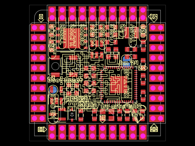 Similar packagetechmannih/imported-rp2350-stamp-boardThis code defines a detailed PCB layout with multiple layers, including the physical outline, component footprints, drilling holes, SMT pads, silkscreen markings, and courtyard outlines for component placement and board edges.
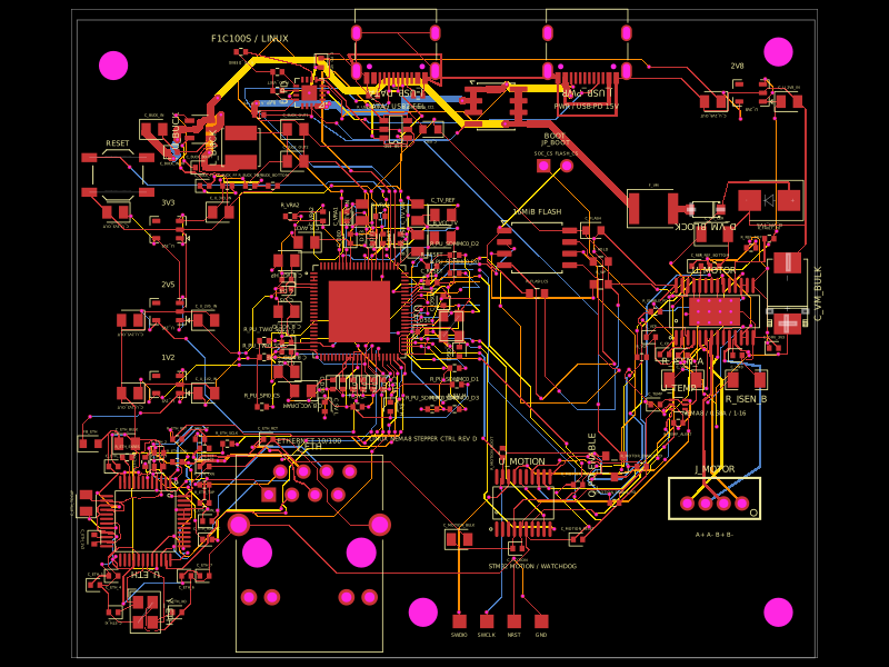 Discover something newshibosoftwaredev/f1c100s-linux-nema8-stepper-controllerRestores component part numbers and CAD models, removes test-point 3D bodies, and validates that solder paste exists only on top-side SMT pads without altering copper or DRC.