mohan-bee/freezer-alarm
This code defines representations of various electronic hardware components—such as voltage regulators, temperature sensors, and microcontroller modules—detailing their physical pins, footprints, and 3D models for PCB design and visualization.
- Version
- 1.0.0
- License
- unset
- Stars
- 0
index.circuit.tsx
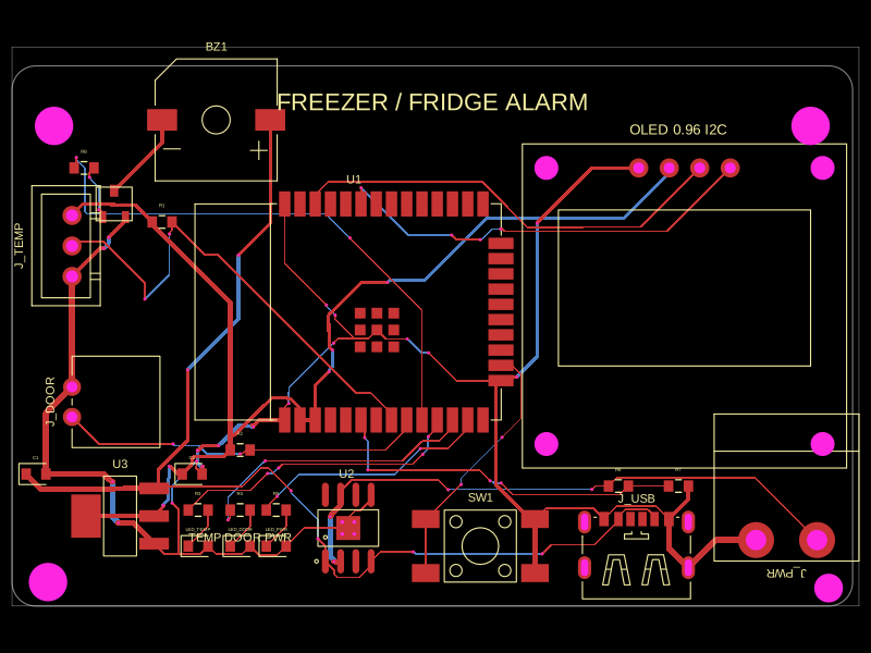
PCB
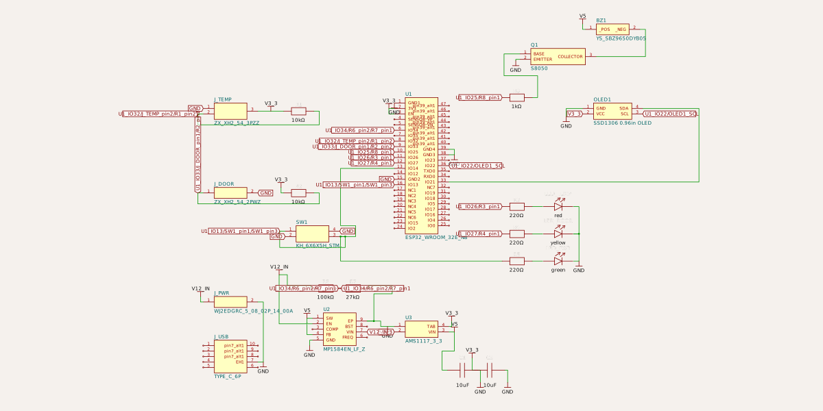
Schematic
import { AMS1117_3_3 } from "./imports/AMS1117_3_3"
import { ESP32_WROOM_32E_N8 } from "./imports/ESP32_WROOM_32E_N8"
import { KH_6X6X5H_STM } from "./imports/KH_6X6X5H_STM"
import { MP1584EN_LF_Z } from "./imports/MP1584EN_LF_Z"
import { TYPE_C_6P } from "./imports/TYPE_C_6P"
import { WJ2EDGRC_5_08_02P_14_00A } from "./imports/WJ2EDGRC_5_08_02P_14_00A"
import { YS_SBZ9650DYB05 } from "./imports/YS_SBZ9650DYB05"
import { ZX_XH2_54_2PWZ } from "./imports/ZX_XH2_54_2PWZ"
import { ZX_XH2_54_3PZZ } from "./imports/ZX_XH2_54_3PZZ"

const ESP32_WROOM_32E_FOOTPRINT = (
  <footprint>
    <silkscreenrect width="18mm" height="25.5mm" pcbX={0} pcbY={0} />
    <silkscreenrect width="14mm" height="6mm" pcbX={0} pcbY={9.2} />
    <smtpad portHints={["pin1"]} pcbX="-9.6mm" pcbY="8mm" width="1.2mm" height="1.1mm" shape="rect" />
    <smtpad portHints={["pin2"]} pcbX="-9.6mm" pcbY="6mm" width="1.2mm" height="1.1mm" shape="rect" />
    <smtpad portHints={["pin3"]} pcbX="-9.6mm" pcbY="4mm" width="1.2mm" height="1.1mm" shape="rect" />
    <smtpad portHints={["pin4"]} pcbX="-9.6mm" pcbY="2mm" width="1.2mm" height="1.1mm" shape="rect" />
    <smtpad portHints={["pin5"]} pcbX="-9.6mm" pcbY="0mm" width="1.2mm" height="1.1mm" shape="rect" />
    <smtpad portHints={["pin6"]} pcbX="-9.6mm" pcbY="-2mm" width="1.2mm" height="1.1mm" shape="rect" />
    <smtpad portHints={["pin7"]} pcbX="-9.6mm" pcbY="-4mm" width="1.2mm" height="1.1mm" shape="rect" />
    <smtpad portHints={["pin8"]} pcbX="-9.6mm" pcbY="-6mm" width="1.2mm" height="1.1mm" shape="rect" />
    <smtpad portHints={["pin9"]} pcbX="-9.6mm" pcbY="-8mm" width="1.2mm" height="1.1mm" shape="rect" />
    <smtpad portHints={["pin10"]} pcbX="9.6mm" pcbY="-8mm" width="1.2mm" height="1.1mm" shape="rect" />
    <smtpad portHints={["pin11"]} pcbX="9.6mm" pcbY="-6mm" width="1.2mm" height="1.1mm" shape="rect" />
    <smtpad portHints={["pin12"]} pcbX="9.6mm" pcbY="-4mm" width="1.2mm" height="1.1mm" shape="rect" />
    <smtpad portHints={["pin13"]} pcbX="9.6mm" pcbY="-2mm" width="1.2mm" height="1.1mm" shape="rect" />
    <smtpad portHints={["pin14"]} pcbX="9.6mm" pcbY="0mm" width="1.2mm" height="1.1mm" shape="rect" />
    <smtpad portHints={["pin15"]} pcbX="9.6mm" pcbY="2mm" width="1.2mm" height="1.1mm" shape="rect" />
    <smtpad portHints={["pin16"]} pcbX="9.6mm" pcbY="4mm" width="1.2mm" height="1.1mm" shape="rect" />
    <smtpad portHints={["pin17"]} pcbX="9.6mm" pcbY="6mm" width="1.2mm" height="1.1mm" shape="rect" />
    <smtpad portHints={["pin18"]} pcbX="9.6mm" pcbY="8mm" width="1.2mm" height="1.1mm" shape="rect" />
  </footprint>
)

const OLED_096_FOOTPRINT = (
  <footprint>
    <silkscreenrect width="27mm" height="27mm" pcbX={0} pcbY={0} />
    <silkscreenrect width="21mm" height="13mm" pcbX={0} pcbY={1.5} />
    <platedhole portHints={["pin1"]} pcbX="-3.81mm" pcbY="11.5mm" outerDiameter="1.6mm" holeDiameter="0.9mm" shape="circle" />
    <platedhole portHints={["pin2"]} pcbX="-1.27mm" pcbY="11.5mm" outerDiameter="1.6mm" holeDiameter="0.9mm" shape="circle" />
    <platedhole portHints={["pin3"]} pcbX="1.27mm" pcbY="11.5mm" outerDiameter="1.6mm" holeDiameter="0.9mm" shape="circle" />
    <platedhole portHints={["pin4"]} pcbX="3.81mm" pcbY="11.5mm" outerDiameter="1.6mm" holeDiameter="0.9mm" shape="circle" />
    <hole pcbX="-11.5mm" pcbY="11.5mm" diameter="2mm" />
    <hole pcbX="11.5mm" pcbY="11.5mm" diameter="2mm" />
    <hole pcbX="-11.5mm" pcbY="-11.5mm" diameter="2mm" />
    <hole pcbX="11.5mm" pcbY="-11.5mm" diameter="2mm" />
  </footprint>
)

const TERMINAL_2P_508_FOOTPRINT = (
  <footprint>
    <silkscreenrect width="10.6mm" height="8mm" pcbX={0} pcbY={0} />
    <platedhole
      portHints={["pin1"]}
      pcbX="-2.54mm"
      pcbY="0mm"
      outerDiameter="2.4mm"
      holeDiameter="1.2mm"
      shape="circle"
    />
    <platedhole
      portHints={["pin2"]}
      pcbX="2.54mm"
      pcbY="0mm"
      outerDiameter="2.4mm"
      holeDiameter="1.2mm"
      shape="circle"
    />
  </footprint>
)

const JST_XH_3P_FOOTPRINT = (
  <footprint>
    <silkscreenrect width="8.5mm" height="6mm" pcbX={0} pcbY={0} />
    <platedhole portHints={["pin1"]} pcbX="-2.5mm" pcbY="0mm" outerDiameter="1.7mm" holeDiameter="1mm" shape="circle" />
    <platedhole portHints={["pin2"]} pcbX="0mm" pcbY="0mm" outerDiameter="1.7mm" holeDiameter="1mm" shape="circle" />
    <platedhole portHints={["pin3"]} pcbX="2.5mm" pcbY="0mm" outerDiameter="1.7mm" holeDiameter="1mm" shape="circle" />
  </footprint>
)

const JST_XH_2P_FOOTPRINT = (
  <footprint>
    <silkscreenrect width="6mm" height="6mm" pcbX={0} pcbY={0} />
    <platedhole portHints={["pin1"]} pcbX="-1.25mm" pcbY="0mm" outerDiameter="1.7mm" holeDiameter="1mm" shape="circle" />
    <platedhole portHints={["pin2"]} pcbX="1.25mm" pcbY="0mm" outerDiameter="1.7mm" holeDiameter="1mm" shape="circle" />
  </footprint>
)

const BUZZER_12MM_FOOTPRINT = (
  <footprint>
    <silkscreencircle radius="6mm" pcbX={0} pcbY={0} />
    <platedhole
      portHints={["pin1"]}
      pcbX="-3.75mm"
      pcbY="0mm"
      outerDiameter="1.8mm"
      holeDiameter="0.9mm"
      shape="circle"
    />
    <platedhole
      portHints={["pin2"]}
      pcbX="3.75mm"
      pcbY="0mm"
      outerDiameter="1.8mm"
      holeDiameter="0.9mm"
      shape="circle"
    />
  </footprint>
)

const AMS1117_SOT223_FOOTPRINT = (
  <footprint>
    <smtpad portHints={["pin1"]} pcbX="-2.3mm" pcbY="-3mm" width="1mm" height="1.7mm" shape="rect" />
    <smtpad portHints={["pin2"]} pcbX="0mm" pcbY="-3mm" width="1mm" height="1.7mm" shape="rect" />
    <smtpad portHints={["pin3"]} pcbX="2.3mm" pcbY="-3mm" width="1mm" height="1.7mm" shape="rect" />
    <smtpad portHints={["pin2"]} pcbX="0mm" pcbY="2.5mm" width="3.8mm" height="3.8mm" shape="rect" />
    <silkscreenrect width="6.5mm" height="7mm" pcbX={0} pcbY={0} />
  </footprint>
)

const XL6009_TO263_5_FOOTPRINT = (
  <footprint>
    <silkscreenrect width="10mm" height="9mm" pcbX={0} pcbY={0} />
    <smtpad portHints={["pin1"]} pcbX="-3.4mm" pcbY="-3.2mm" width="1.1mm" height="2mm" shape="rect" />
    <smtpad portHints={["pin2"]} pcbX="-1.7mm" pcbY="-3.2mm" width="1.1mm" height="2mm" shape="rect" />
    <smtpad portHints={["pin3"]} pcbX="0mm" pcbY="-3.2mm" width="1.1mm" height="2mm" shape="rect" />
    <smtpad portHints={["pin4"]} pcbX="1.7mm" pcbY="-3.2mm" width="1.1mm" height="2mm" shape="rect" />
    <smtpad portHints={["pin5"]} pcbX="3.4mm" pcbY="-3.2mm" width="1.1mm" height="2mm" shape="rect" />
    <smtpad portHints={["pin2"]} pcbX="0mm" pcbY="2.2mm" width="6.5mm" height="4.5mm" shape="rect" />
  </footprint>
)

const SOT23_FOOTPRINT = (
  <footprint>
    <smtpad portHints={["pin1"]} pcbX="-0.95mm" pcbY="-1.1mm" width="0.6mm" height="1mm" shape="rect" />
    <smtpad portHints={["pin2"]} pcbX="0.95mm" pcbY="-1.1mm" width="0.6mm" height="1mm" shape="rect" />
    <smtpad portHints={["pin3"]} pcbX="0mm" pcbY="1.1mm" width="0.7mm" height="1mm" shape="rect" />
    <silkscreenrect width="3mm" height="2.8mm" pcbX={0} pcbY={0} />
  </footprint>
)

const USB_C_POWER_FOOTPRINT = (
  <footprint>
    <silkscreenrect width="9mm" height="7mm" pcbX={0} pcbY={0} />
    <smtpad portHints={["pin1"]} pcbX="-1.8mm" pcbY="2.6mm" width="1.4mm" height="1.8mm" shape="rect" />
    <smtpad portHints={["pin2"]} pcbX="1.8mm" pcbY="2.6mm" width="1.4mm" height="1.8mm" shape="rect" />
    <hole pcbX="-4mm" pcbY="-1.5mm" diameter="1mm" />
    <hole pcbX="4mm" pcbY="-1.5mm" diameter="1mm" />
  </footprint>
)

export default function FreezerFridgeAlarmBoard() {
  return (
    <board width="70mm" height="45mm" layers={2} borderRadius="2mm" title="Freezer / Fridge Alarm">
      <silkscreentext text="FREEZER / FRIDGE ALARM" pcbX={0} pcbY={19.5} fontSize="2mm" anchorAlignment="center" />
      <silkscreentext text="OLED 0.96 I2C" pcbX={20.5} pcbY={17.2} fontSize="1.2mm" anchorAlignment="center" />
      <silkscreentext text="TEMP  DOOR  PWR" pcbX={-16} pcbY={-16.8} fontSize="1mm" anchorAlignment="center" />

      <hole name="H1" diameter="3.2mm" pcbX={-31.5} pcbY={17.5} />
      <hole name="H2" diameter="3.2mm" pcbX={31.5} pcbY={17.5} />
      <hole name="H3" diameter="3.2mm" pcbX={-32} pcbY={-20.5} />
      <hole name="H4" diameter="2.4mm" pcbX={33} pcbY={-21} />

      <ESP32_WROOM_32E_N8
        name="U1"
        pcbX={-3}
        pcbY={2}
        schX={0}
        schY={0}
      />

      <chip
        name="OLED1"
        manufacturerPartNumber="SSD1306 0.96in OLED"
        supplierPartNumbers={{ jlcpcb: ["C152912"] }}
        footprint={OLED_096_FOOTPRINT}
        pcbX={21}
        pcbY={2.5}
        schX={7}
        schY={2}
        pinLabels={{ pin1: "GND", pin2: "VCC", pin3: "SCL", pin4: "SDA" }}
      />

      <ZX_XH2_54_3PZZ
        name="J_TEMP"
        pcbX={-30}
        pcbY={7.5}
        pcbRotation={90}
        schX={-7}
        schY={2}
      />
      <ZX_XH2_54_2PWZ
        name="J_DOOR"
        pcbX={-30}
        pcbY={-5.5}
        pcbRotation={90}
        schX={-7}
        schY={-1}
      />

      <WJ2EDGRC_5_08_02P_14_00A
        name="J_PWR"
        pcbX={29.5}
        pcbY={-17}
        pcbRotation={180}
        schX={-7}
        schY={-5}
      />
      <TYPE_C_6P
        name="J_USB"
        pcbX={17}
        pcbY={-17}
        schX={-7}
        schY={-7}
      />

      <MP1584EN_LF_Z
        name="U2"
        pcbX={-7}
        pcbY={-16}
        schX={-3}
        schY={-6}
      />
      <AMS1117_3_3
        name="U3"
        pcbX={-26}
        pcbY={-15}
        schX={0}
        schY={-6}
      />

      <capacitor name="C1" capacitance="10uF" footprint="0603" supplierPartNumbers={{ jlcpcb: ["C14663"] }} pcbX={-33} pcbY={-11.5} schX={1.5} schY={-7.5} />
      <capacitor name="C2" capacitance="10uF" footprint="0603" supplierPartNumbers={{ jlcpcb: ["C14663"] }} pcbX={-20} pcbY={-11.5} schX={2.5} schY={-7.5} />
      <resistor name="R1" resistance="10k" footprint="0603" supplierPartNumbers={{ jlcpcb: ["C25804"] }} pcbX={-22.5} pcbY={9.5} schX={-4.5} schY={2} />
      <resistor name="R2" resistance="10k" footprint="0603" supplierPartNumbers={{ jlcpcb: ["C25804"] }} pcbX={-16} pcbY={-9.5} schX={-4.5} schY={-1} />
      <resistor name="R3" resistance="220" footprint="0603" supplierPartNumbers={{ jlcpcb: ["C25804"] }} pcbX={-19.5} pcbY={-14.5} schX={3.5} schY={-1.5} />
      <resistor name="R4" resistance="220" footprint="0603" supplierPartNumbers={{ jlcpcb: ["C25804"] }} pcbX={-16} pcbY={-14.5} schX={3.5} schY={-2.5} />
      <resistor name="R5" resistance="220" footprint="0603" supplierPartNumbers={{ jlcpcb: ["C25804"] }} pcbX={-13} pcbY={-14.5} schX={3.5} schY={-3.5} />
      <resistor name="R6" resistance="100k" footprint="0603" pcbX={15.5} pcbY={-12.5} schX={-3.5} schY={-4.5} />
      <resistor name="R7" resistance="27k" footprint="0603" pcbX={20.5} pcbY={-12.5} schX={-2.5} schY={-4.5} />
      <resistor name="R8" resistance="1k" footprint="0603" pcbX={-29} pcbY={14} schX={3.5} schY={2.5} />

      <led name="LED_TEMP" color="red" footprint="0603" supplierPartNumbers={{ jlcpcb: ["C25804"] }} pcbX={-19.5} pcbY={-17.5} schX={5} schY={-1.5} />
      <led name="LED_DOOR" color="yellow" footprint="0603" supplierPartNumbers={{ jlcpcb: ["C25804"] }} pcbX={-16} pcbY={-17.5} schX={5} schY={-2.5} />
      <led name="LED_PWR" color="green" footprint="0603" supplierPartNumbers={{ jlcpcb: ["C25804"] }} pcbX={-13} pcbY={-17.5} schX={5} schY={-3.5} />

      <YS_SBZ9650DYB05
        name="BZ1"
        pcbX={-18}
        pcbY={18}
        schX={7}
        schY={5}
      />
      <chip
        name="Q1"
        manufacturerPartNumber="S8050"
        footprint={SOT23_FOOTPRINT}
        pcbX={-26.5}
        pcbY={11}
        schX={5}
        schY={4}
        pinLabels={{ pin1: "BASE", pin2: "EMITTER", pin3: "COLLECTOR" }}
      />

      <KH_6X6X5H_STM name="SW1" pcbX={4} pcbY={-17.5} schX={-4} schY={-2.5} />

      <trace from="J_PWR.pin1" to="net.V12_IN" width="0.45mm" />
      <trace from="J_PWR.pin2" to="net.GND" width="0.5mm" />
      <trace from="J_USB.A9" to="net.V5" width="0.4mm" />
      <trace from="J_USB.B9" to="net.V5" width="0.4mm" />
      <trace from="J_USB.A12" to="net.GND" width="0.4mm" />
      <trace from="J_USB.B12" to="net.GND" width="0.4mm" />
      <trace from="J_USB.EH1" to="net.GND" width="0.4mm" />
      <trace from="U2.VIN" to="net.V12_IN" width="0.45mm" />
      <trace from="U2.GND" to="net.GND" width="0.45mm" />
      <trace from="U2.EP" to="net.GND" width="0.45mm" />
      <trace from="U2.SW" to="net.V5" width="0.45mm" />
      <trace from="U2.FB" to="net.V5" />
      <trace from="U2.EN" to="net.V12_IN" />
      <trace from="U3.VIN" to="net.V5" width="0.4mm" />
      <trace from="U3.pin1" to="net.GND" />
      <trace from="U3.pin2" to="net.V3_3" width="0.4mm" />
      <trace from="U3.TAB" to="net.V3_3" width="0.4mm" />
      <trace from="C1.pin1" to="net.V5" />
      <trace from="C1.pin2" to="net.GND" />
      <trace from="C2.pin1" to="net.V3_3" />
      <trace from="C2.pin2" to="net.GND" />

      <trace from="U1.3V3" to="net.V3_3" />
      <trace from="U1.GND1" to="net.GND" />
      <trace from="U1.GND2" to="net.GND" />
      <trace from="U1.GND3" to="net.GND" />
      <trace from="U1.GND4" to="net.GND" />
      <trace from="U1.EN" to="net.V3_3" />

      <trace from="OLED1.VCC" to="net.V3_3" />
      <trace from="OLED1.GND" to="net.GND" />
      <trace from="OLED1.SDA" to="U1.IO21" />
      <trace from="OLED1.SCL" to="U1.IO22" />

      <trace from="J_TEMP.pin3" to="net.V3_3" />
      <trace from="J_TEMP.pin1" to="net.GND" />
      <trace from="J_TEMP.pin2" to="U1.IO32" />
      <trace from="R1.pin1" to="net.V3_3" />
      <trace from="R1.pin2" to="J_TEMP.pin2" />

      <trace from="J_DOOR.pin2" to="net.GND" />
      <trace from="J_DOOR.pin1" to="U1.IO33" />
      <trace from="R2.pin1" to="net.V3_3" />
      <trace from="R2.pin2" to="J_DOOR.pin1" />

      <trace from="U1.IO26" to="R3.pin1" />
      <trace from="R3.pin2" to="LED_TEMP.pin1" />
      <trace from="LED_TEMP.pin2" to="net.GND" />
      <trace from="U1.IO27" to="R4.pin1" />
      <trace from="R4.pin2" to="LED_DOOR.pin1" />
      <trace from="LED_DOOR.pin2" to="net.GND" />
      <trace from="U1.IO14" to="R5.pin1" />
      <trace from="R5.pin2" to="LED_PWR.pin1" />
      <trace from="LED_PWR.pin2" to="net.GND" />

      <trace from="BZ1._POS" to="net.V5" width="0.35mm" />
      <trace from="BZ1._NEG" to="Q1.COLLECTOR" width="0.35mm" />
      <trace from="Q1.EMITTER" to="net.GND" />
      <trace from="U1.IO25" to="R8.pin1" />
      <trace from="R8.pin2" to="Q1.BASE" />

      <trace from="SW1.pin1" to="U1.IO13" />
      <trace from="SW1.pin3" to="U1.IO13" />
      <trace from="SW1.pin2" to="net.GND" />
      <trace from="SW1.pin4" to="net.GND" />

      <trace from="R6.pin1" to="net.V12_IN" />
      <trace from="R6.pin2" to="U1.IO34" />
      <trace from="R7.pin1" to="U1.IO34" />
      <trace from="R7.pin2" to="net.GND" />
    </board>
  )
}