krishnax12/ip2312-fast-charging-module
A USB‑C–powered IP2312 single-cell Li‑ion fast-charger board with input/output filtering, selectable charge current jumpers, status LEDs, and VCC/VBAT/GND terminal pads.
- Version
- 0.1.8
- License
- GPL-3.0
- Stars
- 1
index.circuit.tsx
PCB
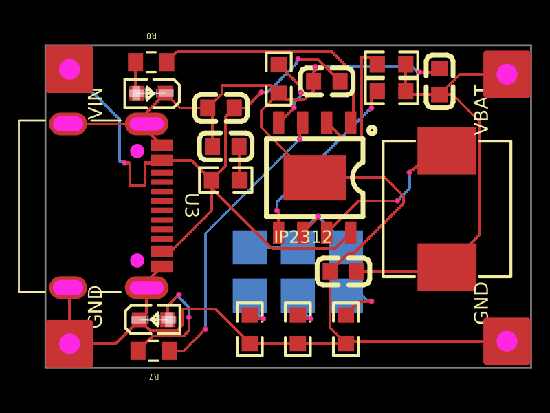
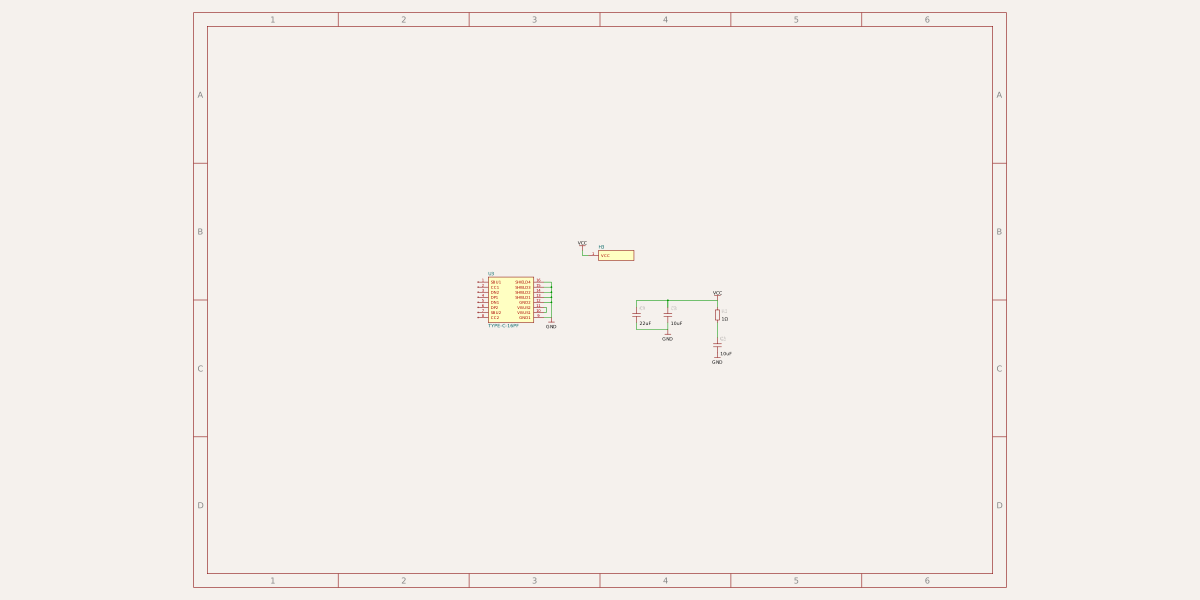
Schematic
import { UsbCInputFootprint } from "./imports/UsbCInputFootprint"

/**
 * IP2312 1-cell lithium battery fast charger
 *
 * Based on Sagar Saini's GPL-3.0 project:
 * https://www.instructables.com/Fast-Charging-Module-for-Lithium-Batteries/
 *
 * Board outline, placement, values, and LCSC references are taken from the
 * published Gerber, CPL, BOM, and schematic files dated 2024-02-08.
 */

const Ip2312 = () => (
  <chip
    name="U1"
    manufacturerPartNumber="IP2312-4V35"
    footprint="jlcpcb:C605433"
    supplierPartNumbers={{ jlcpcb: ["C605433"] }}
    pcbX={1.397}
    pcbY={1.523}
    pcbRotation={180}
    pinLabels={{
      pin1: "CHARGE_LED",
      pin2: "TEST",
      pin3: "STANDBY_LED",
      pin4: "NTC",
      pin5: "BAT",
      pin6: "ICHG",
      pin7: "SW",
      pin8: "VIN",
      pin9: "EP",
    }}
  />
)

const UsbCInput = () => (
  <chip
    name="U3"
    manufacturerPartNumber="TYPE-C-16PF"
    footprint={<UsbCInputFootprint />}
    supplierPartNumbers={{ jlcpcb: ["C2835121"] }}
    cadModel={{
      objUrl:
        "https://modelcdn.tscircuit.com/easyeda_models/download?uuid=c50ce21ae3b941ce8eeb9bccc6cdef41&pn=C2835121",
      rotationOffset: { x: 0, y: 0, z: 180 },
      positionOffset: { x: -2.15, y: 0, z: 0 },
    }}
    pcbX={-8.893}
    pcbY={0.043}
    pcbRotation={270}
    allowOffBoard
    pinLabels={{
      pin1: "SBU1",
      pin2: "CC1",
      pin3: "DN2",
      pin4: "DP1",
      pin5: "DN1",
      pin6: "DP2",
      pin7: "SBU2",
      pin8: "CC2",
      pin9: "GND1",
      pin10: "VBUS1",
      pin11: "VBUS2",
      pin12: "GND2",
      pin13: "SHIELD1",
      pin14: "SHIELD2",
      pin15: "SHIELD3",
      pin16: "SHIELD4",
    }}
  />
)

const TerminalPad = (props: {
  name: string
  label: string
  pcbX: number
  pcbY: number
}) => (
  <chip
    name={props.name}
    pcbX={props.pcbX}
    pcbY={props.pcbY}
    pinLabels={{ pin1: props.label }}
    allowOffBoard
    footprint={
      <footprint>
        <platedhole
          shape="circular_hole_with_rect_pad"
          holeDiameter="1.1mm"
          rectPadWidth="2.5mm"
          rectPadHeight="2.5mm"
          rectBorderRadius="0.15mm"
          portHints={["pin1"]}
        />
      </footprint>
    }
  />
)

const CurrentSelectJumper = (props: { name: string; pcbX: number }) => (
  <solderjumper
    name={props.name}
    pinLabels={{ 1: "CC", 2: "SELECT" }}
    pcbX={props.pcbX}
    pcbY={-3.427}
    pcbRotation={90}
    layer="bottom"
    footprint={
      <footprint>
        <smtpad
          shape="rect"
          width="1.8mm"
          height="1.8mm"
          pcbX={-1.27}
          layer="bottom"
          portHints={["pin1"]}
        />
        <smtpad
          shape="rect"
          width="1.8mm"
          height="1.8mm"
          pcbX={1.27}
          layer="bottom"
          portHints={["pin2"]}
        />
      </footprint>
    }
  />
)

export default () => (
  <board
    width="25.654mm"
    height="17.018mm"
    solderMaskColor="purple"
    autorouter={{ local: true, groupMode: "subcircuit" }}
    schAutoLayoutEnabled
    placementDrcChecksDisabled
  >
    <net name="VCC" isPowerNet />
    <net name="VBAT" isPowerNet />
    <net name="GND" isGroundNet />
    <net name="CC" />
    <net name="SW" />
    <net name="CHARGE_LED" />
    <net name="STANDBY_LED" />

    <schematicsheet
      name="usb_input"
      displayName="USB-C Input and Filtering"
      sheetIndex={0}
    >
      <UsbCInput />
      <capacitor
        name="C1"
        capacitance="22uF"
        footprint="jlcpcb:C59461"
        pcbX={-3.553}
        pcbY={5.203}
        pcbRotation={180}
      />
      <capacitor
        name="C2"
        capacitance="10uF"
        footprint="jlcpcb:C96446"
        pcbX={-3.303}
        pcbY={3.173}
        pcbRotation={180}
      />
      <capacitor
        name="C3"
        capacitance="10uF"
        footprint="jlcpcb:C96446"
        pcbX={2.037}
        pcbY={6.603}
        pcbRotation={180}
      />
      <resistor
        name="R5"
        resistance="1"
        footprint="jlcpcb:C22936"
        pcbX={-3.303}
        pcbY={1.393}
      />
      <TerminalPad name="H3" label="VCC" pcbX={-11.553} pcbY={7.243} />
    </schematicsheet>

    <schematicsheet
      name="charger"
      displayName="IP2312 Charger and Battery Output"
      sheetIndex={1}
    >
      <Ip2312 />
      <inductor
        name="L1"
        inductance="2.2uH"
        footprint="jlcpcb:C385252"
        supplierPartNumbers={{ jlcpcb: ["C385252"] }}
        pcbX={8.387}
        pcbY={-0.127}
        pcbRotation={270}
      />
      <capacitor
        name="C4"
        capacitance="22uF"
        footprint="jlcpcb:C59461"
        pcbX={7.997}
        pcbY={6.603}
        pcbRotation={90}
      />
      <capacitor
        name="C5"
        capacitance="22uF"
        footprint="jlcpcb:C59461"
        pcbX={2.917}
        pcbY={-3.427}
        pcbRotation={180}
      />
      <resistor
        name="R1"
        resistance="51k"
        footprint="jlcpcb:C23196"
        pcbX={-0.503}
        pcbY={6.733}
        pcbRotation={270}
      />
      <resistor
        name="R6"
        resistance="1k"
        footprint="jlcpcb:C3017736"
        pcbX={5.457}
        pcbY={7.5}
      />
      <resistor
        name="R9"
        resistance="1"
        footprint="jlcpcb:C22936"
        pcbX={5.457}
        pcbY={6.093}
      />
      <TerminalPad name="H1" label="VBAT" pcbX={11.557} pcbY={6.983} />
      <TerminalPad name="H4" label="GND" pcbX={11.557} pcbY={-7.107} />
    </schematicsheet>

    <schematicsheet
      name="current_selection"
      displayName="Charge Current Selection"
      sheetIndex={2}
    >
      <resistor
        name="R2"
        resistance="47k"
        footprint="jlcpcb:C25819"
        pcbX={3.047}
        pcbY={-6.477}
        pcbRotation={90}
      />
      <resistor
        name="R3"
        resistance="91k"
        footprint="jlcpcb:C23265"
        pcbX={0.507}
        pcbY={-6.477}
        pcbRotation={90}
      />
      <resistor
        name="R4"
        resistance="130k"
        footprint="jlcpcb:C22795"
        pcbX={-2.033}
        pcbY={-6.477}
        pcbRotation={90}
      />
      <CurrentSelectJumper name="HDR1" pcbX={-2.033} />
      <CurrentSelectJumper name="HDR2" pcbX={0.507} />
      <CurrentSelectJumper name="HDR3" pcbX={3.047} />
      <TerminalPad name="H2" label="GND" pcbX={-11.553} pcbY={-7.237} />
    </schematicsheet>

    <schematicsheet
      name="status_indicators"
      displayName="Charge Status Indicators"
      sheetIndex={3}
    >
      <resistor
        name="R7"
        resistance="100"
        footprint="0603"
        pcbX={-7.113}
        pcbY={-7.617}
        pcbRotation={180}
      />
      <resistor
        name="R8"
        resistance="100"
        footprint="0603"
        pcbX={-7.243}
        pcbY={7.623}
        pcbRotation={180}
      />
      <led
        name="LED1"
        color="red"
        footprint="jlcpcb:C965799"
        pinLabels={{ pin1: "cathode", pin2: "anode" }}
        pcbX={-7.113}
        pcbY={-5.967}
      />
      <led
        name="LED2"
        color="red"
        footprint="jlcpcb:C965799"
        pinLabels={{ pin1: "cathode", pin2: "anode" }}
        pcbX={-7.243}
        pcbY={5.973}
        pcbRotation={180}
      />
    </schematicsheet>

    <silkscreentext
      text="VIN"
      pcbX={-10.2}
      pcbY={5.4}
      pcbRotation={90}
      fontSize="1mm"
    />
    <silkscreentext
      text="GND"
      pcbX={-10.2}
      pcbY={-5.3}
      pcbRotation={90}
      fontSize="1mm"
    />
    <silkscreentext
      text="VBAT"
      pcbX={10.2}
      pcbY={5.1}
      pcbRotation={90}
      fontSize="1mm"
    />
    <silkscreentext
      text="GND"
      pcbX={10.2}
      pcbY={-5.1}
      pcbRotation={90}
      fontSize="1mm"
    />
    <silkscreentext text="IP2312" pcbX={0.8} pcbY={-1.6} fontSize="0.9mm" />
    <trace from=".U3 > .VBUS1" to="net.VCC" />
    <trace from=".U3 > .VBUS2" to="net.VCC" />
    <trace from=".U3 > .GND1" to="net.GND" />
    <trace from=".U3 > .GND2" to="net.GND" />
    <trace from=".U3 > .SHIELD1" to="net.GND" />
    <trace from=".U3 > .SHIELD2" to="net.GND" />
    <trace from=".U3 > .SHIELD3" to="net.GND" />
    <trace from=".U3 > .SHIELD4" to="net.GND" />
    <trace from=".U1 > .VIN" to="net.VCC" />
    <trace from=".U1 > .EP" to="net.GND" />
    <trace from=".U1 > .BAT" to=".R9 > .pin1" />
    <trace from=".R9 > .pin2" to="net.VBAT" />
    <trace from=".U1 > .SW" to="net.SW" />
    <trace from=".L1 > .pin1" to="net.SW" />
    <trace from=".L1 > .pin2" to="net.VBAT" />
    <trace from=".U1 > .ICHG" to="net.CC" />
    <trace from=".U1 > .NTC" to=".R1 > .pin1" />
    <trace from=".R1 > .pin2" to="net.GND" />
    <trace from=".U1 > .TEST" to=".R6 > .pin1" />
    <trace from=".R6 > .pin2" to="net.VBAT" />
    <trace from=".U1 > .CHARGE_LED" to="net.CHARGE_LED" />
    <trace from=".U1 > .STANDBY_LED" to="net.STANDBY_LED" />
    <trace from=".R5 > .pin1" to="net.VCC" />
    <trace from=".R5 > .pin2" to=".C2 > .pin1" />
    <trace from=".C2 > .pin2" to="net.GND" />
    <trace from=".C1 > .pin1" to="net.VCC" />
    <trace from=".C1 > .pin2" to="net.GND" />
    <trace from=".C3 > .pin1" to="net.VCC" />
    <trace from=".C3 > .pin2" to="net.GND" />
    <trace from=".C4 > .pin1" to="net.VBAT" />
    <trace from=".C4 > .pin2" to="net.GND" />
    <trace from=".C5 > .pin1" to="net.VBAT" />
    <trace from=".C5 > .pin2" to="net.GND" />
    <trace from="net.STANDBY_LED" to=".R7 > .pin1" />
    <trace from=".R7 > .pin2" to=".LED1 > .anode" />
    <trace from=".LED1 > .cathode" to="net.GND" />
    <trace from="net.CHARGE_LED" to=".R8 > .pin1" />
    <trace from=".R8 > .pin2" to=".LED2 > .anode" />
    <trace from=".LED2 > .cathode" to="net.GND" />
    <trace from=".R4 > .pin1" to="net.GND" />
    <trace from=".R4 > .pin2" to=".HDR1 > .SELECT" />
    <trace from=".HDR1 > .CC" to="net.CC" />
    <trace from=".R3 > .pin1" to="net.GND" />
    <trace from=".R3 > .pin2" to=".HDR2 > .SELECT" />
    <trace from=".HDR2 > .CC" to="net.CC" />
    <trace from=".R2 > .pin1" to="net.GND" />
    <trace from=".R2 > .pin2" to=".HDR3 > .SELECT" />
    <trace from=".HDR3 > .CC" to="net.CC" />
    <trace from=".H1 > .VBAT" to="net.VBAT" />
    <trace from=".H2 > .GND" to="net.GND" />
    <trace from=".H3 > .VCC" to="net.VCC" />
    <trace from=".H4 > .GND" to="net.GND" />
  </board>
)