imrishabh18/pcbgolf
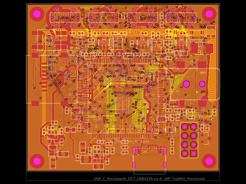
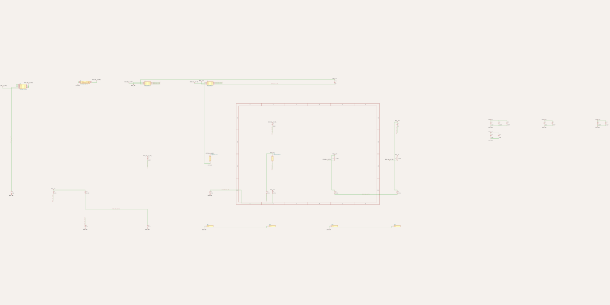
A complete 4-layer PCBGolf controller PCB with STM32H7 MCU, USB/SD and CAN interfaces, power regulation, protection, connectors, switches, LEDs, clocking, and supporting passives.
- Version
- 1.6.1
- License
- unset
- Stars
- 0
index.circuit.tsx
PCB
Schematic
import { Fragment } from "react"
import { cadModelFor, supplierPartNumbersFor } from "./jlcpcb-parts"
import routedCache from "./routed-cache.json"
import { makeSavedAutorouter } from "./saved-autorouter"
import source from "./source-data.json"
import original from "./source-data.original.json"
import population from "./source-population.json"
import layout from "./placement.json"
import boardOutline from "./board-outline.json"
import interfaceLabels from "./interface-labels.json"
import schematicOverrides from "./schematic-overrides.json"
import { footprints, footprintPinMaps } from "./footprints"
import type { PinAttributeMap } from "@tscircuit/props"

/** Complete original PCBGolf circuit. All 191 connected nets come from the source PCB. */
const sections = ["Power", "STM32H7", "USB + SD", "CAN-FD", "Channels"]
const schematic: Record<string, { x: number; y: number; height: number; section: string }> = {}
// Preserve the reviewed sheet order when a corrected package has fewer pins.
const originalPadCounts = new Map(original.components.filter(c => c.ref === "J3")
  .map(c => [c.ref, c.pads.length]))
for (const [si, section] of sections.entries()) {
  const parts = source.components.filter(c => c.sheet === section)
    .sort((a, b) => (originalPadCounts.get(b.ref) ?? b.pads.length) -
                   (originalPadCounts.get(a.ref) ?? a.pads.length))
  let col = 0, y = 0, rowHeight = 0
  for (const c of parts) {
    const count = Object.keys(footprintPinMaps[c.footprint]).length
    const height = Math.max(1.6, Math.ceil(count / 2) * 0.7)
    if (col >= 7) { y -= rowHeight + 6; col = 0; rowHeight = 0 }
    schematic[c.ref] = {x: col * 14, y: y - height / 2, height, section: `S${si}`}
    rowHeight = Math.max(rowHeight, height)
    col++
  }
}
// Supply roles follow the source circuit. Inductors and Q1 pass power from the
// preceding stage; the switched OBD-C supplies remain four separate nets.
const powerProviders: Record<string, string> = {
  "Net-(J1-PWR)": "J1", "+12V": "Q1", "+5V": "L2", "+3V3": "L1",
  "VBUS": "J3", "VDDA": "L3", "VDDLDO": "L4", "VLXSMPS": "U3",
  "Net-(U1-SW)": "U1", "Net-(U2-SW)": "U2",
  "Net-(U4-VDD18)": "U4", "Net-(U4-VDD18PLL)": "U4",
  ...Object.fromEntries(Array.from({length:4}, (_,i) =>
    [`Net-(J${i+5}-VBUS-PadA4)`, `U${i+13}`])),
}
const powerNets = new Set(Object.keys(powerProviders))
const phaseFor = (name: string) => name === "GND" ? 0 :
  /D_[NP]$|USB[12]?_D[MP]/.test(name) ? 1 :
  /OSC|XTAL/.test(name) ? 2 : powerNets.has(name) ? 4 : 3
const powerWidths: Record<string, number> = {
  "Net-(J1-PWR)":2, "+12V":2, "+5V":0.6, "+3V3":0.4, "GND":0.2,
  "VBUS":0.4, "VDDA":0.4, "VDDLDO":0.6, "VLXSMPS":0.6,
  "Net-(U1-SW)":1.5, "Net-(U2-SW)":1.5,
  "Net-(U4-VDD18)":0.4, "Net-(U4-VDD18PLL)":0.4,
  ...Object.fromEntries(Array.from({length:4},(_,i)=>[`Net-(J${i+5}-VBUS-PadA4)`,1])),
}
const voltageRailNets = new Set([...powerNets].filter(n =>
  !["VLXSMPS", "Net-(U1-SW)", "Net-(U2-SW)"].includes(n)))

const pinAttributesFor = (c: typeof source.components[number]) => {
  const pinMap = footprintPinMaps[c.footprint]
  const attributes: Record<string, PinAttributeMap> = {}
  for (const [sourcePin, pin] of Object.entries(pinMap)) {
    const nets = c.pads.filter(p => p.pin === sourcePin).map(p => p.net)
      .filter((n): n is string => !!n)
    if (nets.length > 0 && nets.every(n => n.startsWith("unconnected-"))) {
      attributes[pin] = {doNotConnect:true}
    } else if (nets.includes("GND")) {
      attributes[pin] = c.ref === "J1" ? {providesGround:true} : {requiresGround:true}
    } else {
      const powerNet = nets.find(n => powerNets.has(n))
      if (powerNet) attributes[pin] = powerProviders[powerNet] === c.ref
        ? {providesPower:true} : {requiresPower:true}
    }
  }
  return attributes
}

const passiveSchematicRotation = (c: typeof source.components[number]) => {
  const groundPin = c.pads.find(p => p.net === "GND")?.pin
  if (groundPin) return groundPin === "1" ? 90 : -90
  const railPin = c.pads.find(p => p.net && voltageRailNets.has(p.net))?.pin
  return railPin ? (railPin === "1" ? -90 : 90) : 0
}

const resistanceFromSource = (value: string): number | string => {
  if (/^0R$/i.test(value)) return 0
  return value.replace(/^(\d+)([kKMmRr])(\d+)$/, (_,whole,unit,fraction) =>
    `${whole}.${fraction}${/[Rr]/.test(unit) ? "" : unit === "K" ? "k" : unit}`)
}

const capacitanceFromSource = (value: string): number | string => {
  // C6/C10 have no nominal capacitance or MPN in the source. Zero represents
  // their absent capacitance with doNotPlace=true, not a selected 0 F part.
  if (value === "DNP") return 0
  return value.endsWith("F") ? value : `${value}F`
}

// Explicit local schematic banks for the physically distributed supply bypasses.
// Their zero PCB transforms preserve all authored component coordinates.
const schematicBanks = [
  {
    "name": "MCU_VDD_Original",
    "title": "U3 VDD: bulk and original bypass",
    "sheet": "STM32H7",
    "refs": [
      "C19",
      "C20",
      "C23",
      "C24",
      "C26",
      "C27"
    ]
  },
  {
    "name": "MCU_VDD_LowPins",
    "title": "U3 VDD: pins 7, 8, 19, 32, 56, 71",
    "sheet": "STM32H7",
    "refs": [
      "C54",
      "C63",
      "C55",
      "C56",
      "C57",
      "C58"
    ]
  },
  {
    "name": "MCU_VDD_HighPins",
    "title": "U3 VDD: pins 91, 92, 106, 119, 144",
    "sheet": "STM32H7",
    "refs": [
      "C64",
      "C59",
      "C60",
      "C61",
      "C62"
    ]
  },
  {
    "name": "Hub_VDD_Original",
    "title": "U4 VDD: bulk and original bypass",
    "sheet": "USB + SD",
    "refs": [
      "C30",
      "C31",
      "C37"
    ]
  },
  {
    "name": "Hub_VDD_Local",
    "title": "U4 VDD: pins 5, 10, 46, 57, 64",
    "sheet": "USB + SD",
    "refs": [
      "C65",
      "C66",
      "C67",
      "C68",
      "C69"
    ]
  }
]
const bankReferences = new Set(schematicBanks.flatMap(bank => bank.refs))
const renderComponent = (c: typeof source.components[number]) => {
      const p = layout.components[c.ref as keyof typeof layout.components]
      const sch = schematic[c.ref]
      const pinMap = footprintPinMaps[c.footprint]
      const so = (schematicOverrides as Record<string, {schX?:number;schY?:number;schHeight?:number;rotationDelta?:number}>)[c.ref] || {}
      // The GCT USB2 connector combines these A/B power contacts on four lands.
      // The legacy branch is retained only for reproducible original-source audits.
      const internallyConnectedPins = c.ref === "J3" ? (c.footprint.startsWith("USB_C_Receptacle_GCT_USB4105")
        ? [["A1","B12"], ["A4","B9"], ["A9","B4"], ["A12","B1"]] : [
        ...Array.from({length:12}, (_,i) => [`B${i+1}`, `B${i+1}T`]),
        ...Array.from({length:4}, (_,i) => [`S${i+1}B`, `S${i+1}T`, `S${i+1}TH`]),
      ]).map(ids => ids.map(id => pinMap[id])) : undefined
      const doNotPlace = (population.components as Record<string, {doNotPopulate:boolean}>)[c.ref]?.doNotPopulate ?? false
      const props = { name:c.ref,
        cadModel: doNotPlace ? undefined : cadModelFor(c.ref),
        supplierPartNumbers: supplierPartNumbersFor(c.ref),
        manufacturerPartNumber:c.properties.MPN || (doNotPlace ? undefined : c.value),
        doNotPlace,
        footprint:footprints[c.footprint as keyof typeof footprints](),
        pinAttributes:pinAttributesFor(c),
        pcbX:p.x, pcbY:p.y, pcbRotation:p.rotation,
        // Mixed-side J3 shield lands must retain their authored footprint layers.
        // An explicit top component layer overrides these in core 0.0.2506.
        layer:(p as {layer?:"top"|"bottom"}).layer === "bottom" ? "bottom" : undefined,
        schX:so.schX ?? sch.x, schY:so.schY ?? sch.y, schHeight:so.schHeight,
        schSectionName:sch.section, schSheetName:c.sheet, schPinSpacing:0.7 }
      if (/^R\d+$/.test(c.ref)) return <resistor key={c.ref} {...props}
        resistance={resistanceFromSource(c.value)} schRotation={passiveSchematicRotation(c)+(so.rotationDelta || 0)} />
      if (/^C\d+$/.test(c.ref)) return <capacitor key={c.ref} {...props}
        capacitance={capacitanceFromSource(c.value)} doNotPlace={doNotPlace}
        schRotation={passiveSchematicRotation(c)+(so.rotationDelta || 0)} />
      if (["L1", "L2", "L4"].includes(c.ref)) return <inductor key={c.ref} {...props}
        inductance={c.value.replace(/^(\d+)u(\d+)$/, "$1.$2uH")} schRotation={passiveSchematicRotation(c)} />
      const pins = Object.values(pinMap)
      const groundSourcePin = c.pads.find(p => p.net === "GND")?.pin
      const railSourcePin = c.pads.find(p => p.net && voltageRailNets.has(p.net))?.pin
      const bottom = groundSourcePin ? pinMap[groundSourcePin] :
        railSourcePin ? pins.find(p => p !== pinMap[railSourcePin]) : undefined
      const schPinArrangement = pins.length === 2 && bottom ? {
        topSide: pins.filter(p => p !== bottom), bottomSide:[bottom],
        leftSide:[], rightSide:[],
      } : undefined
      const chipProps = { ...props, internallyConnectedPins, schRotation:0, schPinArrangement,
        schWidth:schPinArrangement ? 0.4 : undefined,
        pinLabels:Object.fromEntries(Object.entries(pinMap).map(([id,pin])=>[pin, `P_${id.replace(/[^A-Za-z0-9_]/g,"_")}`])) }
      return c.ref.startsWith("J") ? <connector key={c.ref} {...chipProps} /> : <chip key={c.ref} {...chipProps} />

}

export default function PCBGolf() {
  return <board width={layout.width} height={layout.height} outline={boardOutline.points} layers={4} thickness={1.6}
    title="PCBGolf — complete controller" minTraceWidth={0.095} nominalTraceWidth={0.1524}
    minViaPadDiameter={0.3} minViaHoleDiameter={0.15} autorouterEffortLevel="2x"
    minBoardEdgeClearance={0.3} minViaHoleEdgeToViaHoleEdgeClearance={0.25}
    minPlatedHoleDrillEdgeToDrillEdgeClearance={0.45} minPadEdgeToPadEdgeClearance={0.15}
    schTraceAutoLabelEnabled schMaxTraceDistance={1}>
    {sections.map((s,i) => <schematicsheet name={s} displayName={s} sheetIndex={i} />)}
    {sections.map((s,i) => <schematicsection name={`S${i}`} displayName={s} />)}
    {source.components.filter(c => !bankReferences.has(c.ref)).map(renderComponent)}
    {schematicBanks.map(bank => <group key={bank.name} name={bank.name}
      schTitle={bank.title} schSheetName={bank.sheet}
      pcbX={0} pcbY={0} pcbLayout={{layoutMode:"none"}}
      schX={0} schY={0} schLayout={{layoutMode:"none"}}>
      {bank.refs.map(ref => renderComponent(source.components.find(c => c.ref === ref)!))}
      <schematictext text={bank.title} fontSize={0.24} anchor="bottom_left"
        schX={(schematicOverrides as Record<string, {schX?:number}>)[bank.refs[0]].schX! - 0.5}
        schY={(schematicOverrides as Record<string, {schY?:number}>)[bank.refs[0]].schY! + 1.8} />
    </group>)}
    {source.nets.map(n => <net name={n.name} routingPhaseIndex={phaseFor(n.originalName)}
      isGroundNet={n.originalName === "GND"} isPowerNet={powerNets.has(n.originalName)} />)}
    {/* Filled ground is verified across individual copper islands in the native
        board. A shared net name alone is not treated as physical continuity. */}
    {(["top", "inner1", "inner2", "bottom"] as const).map(layer =>
      <copperpour key={layer} name={`Ground ${layer}`} layer={layer}
        connectsTo={`net.${source.nets.find(n => n.originalName === "GND")!.name}`}
        clearance={0.105} boardEdgeMargin={0.3} useThermalReliefs={false} />)}
    {/* Each trace represents a complete branched net. The core otherwise copies
        a capacitor's automatic 1 mm local bypass limit onto the entire network,
        including remote connectors. This conservative network budget bounds the
        branched route; local bypass lengths are audited separately by target. */}
    {source.nets.map(n => <trace key={n.name} name={`T_${n.name}`} schDisplayLabel={n.originalName}
      maxLength={n.pins.length * Math.hypot(layout.width, layout.height)}
      thickness={/D_[NP]$/.test(n.originalName) ? 0.247396 : powerWidths[n.originalName] ?? 0.1524}
      path={[...n.pins.map(p => {
        const c=source.components.find(c=>c.ref===p.ref)!
        return `${p.ref}.${footprintPinMaps[c.footprint][p.pin]}`
      }), `net.${n.name}`]} routingPhaseIndex={phaseFor(n.originalName)} />)}
    <autoroutingphase name="Ground fanout" phaseIndex={0} autorouter={makeSavedAutorouter(routedCache)} />
    <autoroutingphase name="USB" phaseIndex={1} autorouter={makeSavedAutorouter(routedCache)} />
    <autoroutingphase name="Clock" phaseIndex={2} autorouter={makeSavedAutorouter(routedCache)} />
    <autoroutingphase name="Signals" phaseIndex={3} autorouter={makeSavedAutorouter(routedCache)} />
    <autoroutingphase name="Power routing" phaseIndex={4} autorouter={makeSavedAutorouter(routedCache)} />
    {interfaceLabels.map(label => <Fragment key={label.text}><silkscreentext text={label.text}
      pcbX={label.x} pcbY={label.y} pcbRotation={label.rotation} fontSize={label.fontSize} /></Fragment>)}
  </board>
}