gokul/usb3-sd-hub
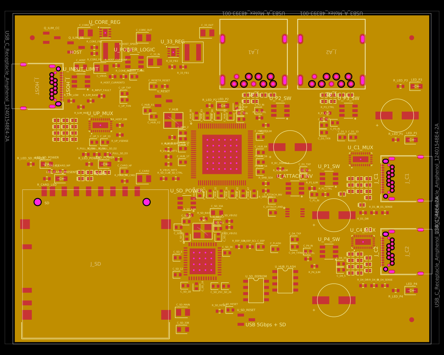
Engineering draft: four-layer, computer-powered USB 3 hub with one USB-C host socket, two USB-C and two USB-A accessory sockets, and a full-size SD slot. Board and three schematic previews are available. Routing and production checks are incomplete; not fabrication ready.
- Version
- 0.1.4
- License
- unset
- Stars
- 0
verification/JLCPCB-STACKUP.md
PCB
Schematic

# Manufacturing profile selected by the user

JLCPCB, four copper layers, nominal 1.6 mm, controlled impedance. No order has been placed.

The official JLCPCB calculator was checked on 2026-10-11 with 1 oz outer copper, 0.5 oz inner copper, L1 signal / L2 reference, non-coplanar differential pair, 90 Ω, and 5.9055 mil pair spacing. For **JLC04161H-3313**, it returned **5.3400 mil trace width / 5.9100 mil spacing** (0.135636 mm / 0.150114 mm). The source uses 0.136 mm / 0.150 mm. The calculator lists nominal finished thickness 1.56 mm ±10% for this 1.6 mm profile.

Stackup: L1 copper 0.035 mm; 3313 prepreg 0.0994 mm; L2 copper 0.0152 mm; core 1.265 mm; L3 copper 0.0152 mm; 3313 prepreg 0.0994 mm; L4 copper 0.035 mm. L2 and L3 are intended ground references. Pair routes must be on outer copper and must be checked for intact references, pad transitions, coupling, and actual skew before release.

Manufacturing request: 90 Ω differential ±10%, approved stackup JLC04161H-3313, impedance coupon. The calculator's 0.5% numerical search tolerance is not a fabrication tolerance. JLCPCB must confirm the finished stackup and controlled-impedance dimensions; no impedance report exists for an unmanufactured board.

This records the selected fabrication target. It is not a fabrication release or proof that every generated route conforms to it.

Sources: [JLCPCB stackups](https://jlcpcb.com/impedance), [official calculator](https://jlcpcb.com/pcb-impedance-calculator). Screenshot: `jlcpcb-impedance-calculator.png`.
Related Packages
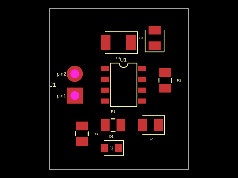 More from this authorgokul/led-blinkingThis design implements a hardware LED blink circuit using a 555 timer IC connected with resistors, capacitors, an LED, and header pins for power input.
 Similar packagepixalynx/usb3-hub-10gA USB 3.2 Gen 2 six-port hub board with USB-C PD power input, regulated 5 V/3.3 V/1.15 V rails, one upstream and four protected downstream USB-A/USB-C ports, SuperSpeed muxes, ESD protection, and controlled port power.
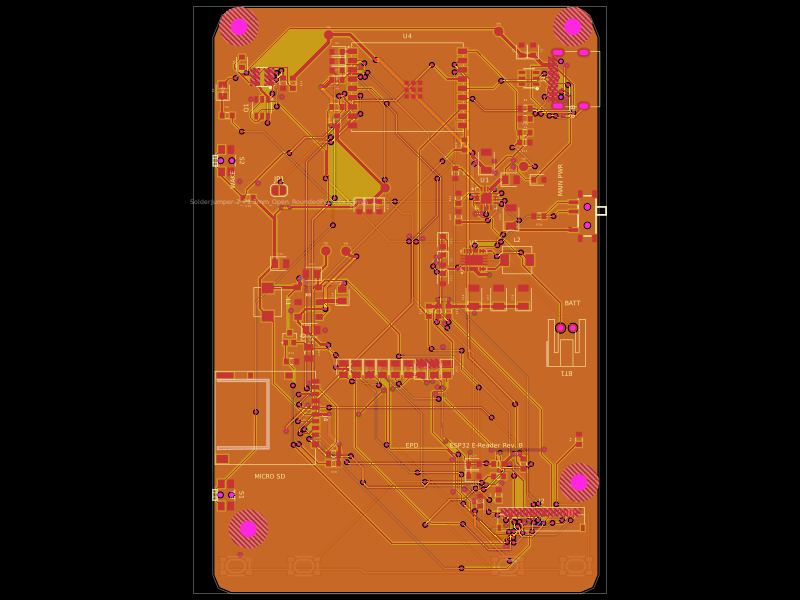 Discover something newrushabhcodes/ESP32-E-ReaderA compact ESP32-C3 board with USB-C power/charging, Li-ion battery protection, 3.3-V regulation, e-paper and microSD interfaces, and user buttons/switches.