gokul/usb3-sd-hub
Engineering draft: four-layer, computer-powered USB 3 hub with one USB-C host socket, two USB-C and two USB-A accessory sockets, and a full-size SD slot. Board and three schematic previews are available. Routing and production checks are incomplete; not fabrication ready.
- Version
- 0.1.5
- License
- MIT
- Stars
- 0
imports/TPS2553DBVR.tsx
import { SchematicNote } from "../components/SchematicNote";
import { placementFor } from "../design/placement";
import type { ChipProps } from "@tscircuit/props";

const pinLabels = {
	pin1: ["IN"],
	pin2: ["GND"],
	pin3: ["EN"],
	pin4: ["FAULT"],
	pin5: ["ILIM"],
	pin6: ["OUT"],
} as const;

const pinAttributes = {
	pin1: { requiresPower: true },
	pin6: { providesPower: true },
	pin2: { requiresGround: true },
} as const;

export const TPS2553DBVR = (props: ChipProps<typeof pinLabels>) => {
	return (
		<chip
			pinLabels={pinLabels}
			pinAttributes={pinAttributes}
			supplierPartNumbers={{
				jlcpcb: ["C55266"],
			}}
			manufacturerPartNumber="TPS2553DBVR"
			footprint={
				<footprint>
					<smtpad
						portHints={["pin3"]}
						pcbX="1.35001mm"
						pcbY="0.94996mm"
						width="1.0999978mm"
						height="0.5999988mm"
						shape="rect"
					/>
					<smtpad
						portHints={["pin2"]}
						pcbX="1.35001mm"
						pcbY="-0mm"
						width="1.0999978mm"
						height="0.5999988mm"
						shape="rect"
					/>
					<smtpad
						portHints={["pin1"]}
						pcbX="1.35001mm"
						pcbY="-0.94996mm"
						width="1.0999978mm"
						height="0.5999988mm"
						shape="rect"
					/>
					<smtpad
						portHints={["pin6"]}
						pcbX="-1.35001mm"
						pcbY="-0.94996mm"
						width="1.0999978mm"
						height="0.5999988mm"
						shape="rect"
					/>
					<smtpad
						portHints={["pin5"]}
						pcbX="-1.35001mm"
						pcbY="-0mm"
						width="1.0999978mm"
						height="0.5999988mm"
						shape="rect"
					/>
					<smtpad
						portHints={["pin4"]}
						pcbX="-1.35001mm"
						pcbY="0.94996mm"
						width="1.0999978mm"
						height="0.5999988mm"
						shape="rect"
					/>
					<silkscreenpath
						route={[
							{ x: -0.899998200000141, y: 1.5499080000000731 },
							{ x: 0.9000236000000541, y: 1.5499080000000731 },
						]}
					/>
					<silkscreenpath
						route={[
							{ x: -0.899998200000141, y: -1.5501111999999466 },
							{ x: 0.9000236000000541, y: -1.5501111999999466 },
						]}
					/>
					<silkscreencircle pcbX="1.397mm" pcbY="-1.651mm" radius="0.127mm" />
					<silkscreentext
						text="{NAME}"
						pcbX="0.012446mm"
						pcbY="2.562354mm"
						anchorAlignment="center"
						fontSize="1mm"
					/>
					<courtyardoutline
						outline={[
							{ x: -2.150008899999989, y: 1.6999081999999817 },
							{ x: 2.150008899999989, y: 1.6999081999999817 },
							{ x: 2.150008899999989, y: -1.700085999999942 },
							{ x: -2.150008899999989, y: -1.700085999999942 },
							{ x: -2.150008899999989, y: 1.6999081999999817 },
						]}
					/>
				</footprint>
			}
			cadModel={{
				objUrl:
					"https://modelcdn.tscircuit.com/easyeda_models/assets/C55266.obj?uuid=229b69761e2c45dba6a83d8866dec72d",
				stepUrl:
					"https://modelcdn.tscircuit.com/easyeda_models/assets/C55266.step?uuid=229b69761e2c45dba6a83d8866dec72d",
				pcbRotationOffset: 180,
				modelOriginPosition: {
					x: 0.000025399999913133797,
					y: -0.0000889000000370288,
					z: -0.048939,
				},
			}}
			{...props}
			{...placementFor(props.name)}
		>
			<SchematicNote
				text={"Current-limited power switch\n2.5–6.5 V; resistor-set limit"}
			/>
		</chip>
	);
};
Related Packages
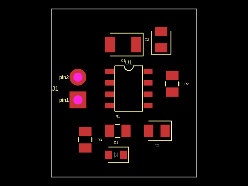 More from this authorgokul/led-blinkingThis design implements a hardware LED blink circuit using a 555 timer IC connected with resistors, capacitors, an LED, and header pins for power input.
 Similar packagepixalynx/usb3-hub-10gA USB 3.2 Gen 2 six-port hub board with USB-C PD power input, regulated 5 V/3.3 V/1.15 V rails, one upstream and four protected downstream USB-A/USB-C ports, SuperSpeed muxes, ESD protection, and controlled port power.
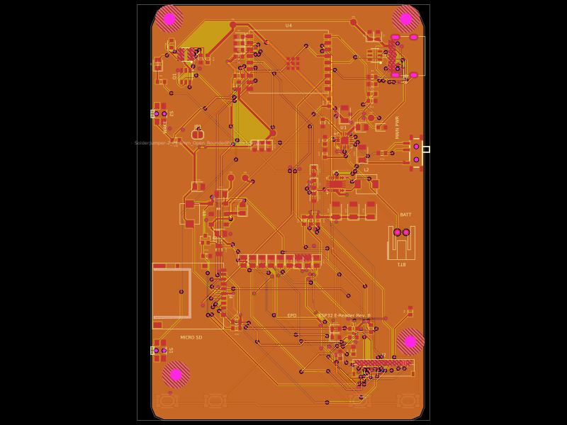 Discover something newrushabhcodes/ESP32-E-ReaderA compact ESP32-C3 board with USB-C power/charging, Li-ion battery protection, 3.3-V regulation, e-paper and microSD interfaces, and user buttons/switches.