gokul/usb3-sd-hub
Engineering draft: four-layer, computer-powered USB 3 hub with one USB-C host socket, two USB-C and two USB-A accessory sockets, and a full-size SD slot. Board and three schematic previews are available. Routing and production checks are incomplete; not fabrication ready.
- Version
- 0.1.5
- License
- MIT
- Stars
- 0
footprints/USB_C_Receptacle_Amphenol_12401548E4-2A.kicad_mod
(module USB_C_Receptacle_Amphenol_12401548E4-2A (layer F.Cu) (tedit 5A142044)
  (descr "USB TYPE C, RA RCPT PCB, Hybrid, https://www.amphenolcanada.com/StockAvailabilityPrice.aspx?From=&PartNum=12401548E4%7e2A")
  (tags "USB C Type-C Receptacle Hybrid")
  (attr smd)
  (fp_text reference REF** (at 0 -6.36) (layer F.SilkS)
    (effects (font (size 1 1) (thickness 0.15)))
  )
  (fp_text value USB_C_Receptacle_Amphenol_12401548E4-2A (at 0 6.14) (layer F.Fab)
    (effects (font (size 1 1) (thickness 0.15)))
  )
  (fp_text user %R (at 0 0) (layer F.Fab)
    (effects (font (size 1 1) (thickness 0.1)))
  )
  (fp_line (start -5.39 5.73) (end -5.39 -5.87) (layer F.CrtYd) (width 0.05))
  (fp_line (start 5.39 5.73) (end -5.39 5.73) (layer F.CrtYd) (width 0.05))
  (fp_line (start 5.39 -5.87) (end 5.39 5.73) (layer F.CrtYd) (width 0.05))
  (fp_line (start -5.39 -5.87) (end 5.39 -5.87) (layer F.CrtYd) (width 0.05))
  (fp_line (start 4.6 5.23) (end 4.6 -5.22) (layer F.Fab) (width 0.1))
  (fp_line (start -4.6 5.23) (end 4.6 5.23) (layer F.Fab) (width 0.1))
  (fp_line (start 3.25 -5.37) (end 4.75 -5.37) (layer F.SilkS) (width 0.12))
  (fp_line (start 4.75 -5.37) (end 4.75 1.89) (layer F.SilkS) (width 0.12))
  (fp_line (start -4.75 -5.37) (end -4.75 1.89) (layer F.SilkS) (width 0.12))
  (fp_line (start -4.75 -5.37) (end -3.25 -5.37) (layer F.SilkS) (width 0.12))
  (fp_line (start -4.6 -5.22) (end 4.6 -5.22) (layer F.Fab) (width 0.1))
  (fp_line (start -4.6 5.23) (end -4.6 -5.22) (layer F.Fab) (width 0.1))
  (pad S1 thru_hole oval (at -4.13 -3.11) (size 0.8 1.4) (drill oval 0.5 1.1) (layers *.Cu *.Mask))
  (pad A1 smd rect (at -2.75 -5.02) (size 0.3 0.7) (layers F.Cu F.Paste F.Mask))
  (pad A2 smd rect (at -2.25 -5.02) (size 0.3 0.7) (layers F.Cu F.Paste F.Mask))
  (pad A3 smd rect (at -1.75 -5.02) (size 0.3 0.7) (layers F.Cu F.Paste F.Mask))
  (pad A4 smd rect (at -1.25 -5.02) (size 0.3 0.7) (layers F.Cu F.Paste F.Mask))
  (pad A5 smd rect (at -0.75 -5.02) (size 0.3 0.7) (layers F.Cu F.Paste F.Mask))
  (pad A6 smd rect (at -0.25 -5.02) (size 0.3 0.7) (layers F.Cu F.Paste F.Mask))
  (pad A7 smd rect (at 0.25 -5.02) (size 0.3 0.7) (layers F.Cu F.Paste F.Mask))
  (pad A12 smd rect (at 2.75 -5.02) (size 0.3 0.7) (layers F.Cu F.Paste F.Mask))
  (pad A10 smd rect (at 1.75 -5.02) (size 0.3 0.7) (layers F.Cu F.Paste F.Mask))
  (pad A9 smd rect (at 1.25 -5.02) (size 0.3 0.7) (layers F.Cu F.Paste F.Mask))
  (pad A8 smd rect (at 0.75 -5.02) (size 0.3 0.7) (layers F.Cu F.Paste F.Mask))
  (pad A11 smd rect (at 2.25 -5.02) (size 0.3 0.7) (layers F.Cu F.Paste F.Mask))
  (pad S1 thru_hole oval (at 4.13 -3.11) (size 0.8 1.4) (drill oval 0.5 1.1) (layers *.Cu *.Mask))
  (pad S1 thru_hole oval (at 4.49 2.84) (size 0.8 1.4) (drill oval 0.5 1.1) (layers *.Cu *.Mask))
  (pad S1 thru_hole oval (at -4.49 2.84) (size 0.8 1.4) (drill oval 0.5 1.1) (layers *.Cu *.Mask))
  (pad "" np_thru_hole oval (at 3.6 -4.36) (size 0.95 0.65) (drill oval 0.95 0.65) (layers *.Cu *.Mask))
  (pad "" np_thru_hole circle (at -3.6 -4.36) (size 0.65 0.65) (drill 0.65) (layers *.Cu *.Mask))
  (pad B1 thru_hole circle (at 2.8 -3.71) (size 0.65 0.65) (drill 0.4) (layers *.Cu *.Mask))
  (pad B4 thru_hole circle (at 1.2 -3.71) (size 0.65 0.65) (drill 0.4) (layers *.Cu *.Mask))
  (pad B6 thru_hole circle (at 0.4 -3.71) (size 0.65 0.65) (drill 0.4) (layers *.Cu *.Mask))
  (pad B7 thru_hole circle (at -0.4 -3.71) (size 0.65 0.65) (drill 0.4) (layers *.Cu *.Mask))
  (pad B9 thru_hole circle (at -1.2 -3.71) (size 0.65 0.65) (drill 0.4) (layers *.Cu *.Mask))
  (pad B12 thru_hole circle (at -2.8 -3.71) (size 0.65 0.65) (drill 0.4) (layers *.Cu *.Mask))
  (pad B2 thru_hole circle (at 2.4 -3.01) (size 0.65 0.65) (drill 0.4) (layers *.Cu *.Mask))
  (pad B3 thru_hole circle (at 1.6 -3.01) (size 0.65 0.65) (drill 0.4) (layers *.Cu *.Mask))
  (pad B5 thru_hole circle (at 0.8 -3.01) (size 0.65 0.65) (drill 0.4) (layers *.Cu *.Mask))
  (pad B8 thru_hole circle (at -0.8 -3.01) (size 0.65 0.65) (drill 0.4) (layers *.Cu *.Mask))
  (pad B10 thru_hole circle (at -1.6 -3.01) (size 0.65 0.65) (drill 0.4) (layers *.Cu *.Mask))
  (pad B11 thru_hole circle (at -2.4 -3.01) (size 0.65 0.65) (drill 0.4) (layers *.Cu *.Mask))
  (model ${KISYS3DMOD}/Connector_USB.3dshapes/USB_C_Receptacle_Amphenol_12401548E4-2A.wrl
    (at (xyz 0 0 0))
    (scale (xyz 1 1 1))
    (rotate (xyz 0 0 0))
  )
)
Related Packages
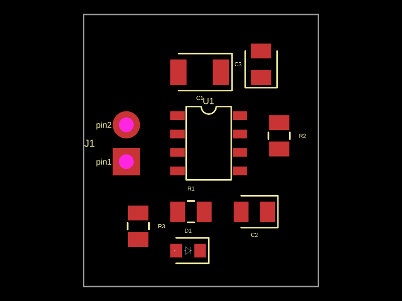 More from this authorgokul/led-blinkingThis design implements a hardware LED blink circuit using a 555 timer IC connected with resistors, capacitors, an LED, and header pins for power input.
 Similar packagepixalynx/usb3-hub-10gA USB 3.2 Gen 2 six-port hub board with USB-C PD power input, regulated 5 V/3.3 V/1.15 V rails, one upstream and four protected downstream USB-A/USB-C ports, SuperSpeed muxes, ESD protection, and controlled port power.
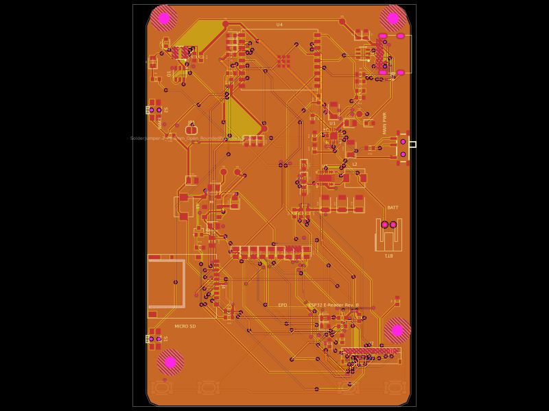 Discover something newrushabhcodes/ESP32-E-ReaderA compact ESP32-C3 board with USB-C power/charging, Li-ion battery protection, 3.3-V regulation, e-paper and microSD interfaces, and user buttons/switches.