anil08607/Smartwatch
A 46 mm smartwatch PCB built around an nRF52810 BLE MCU, with USB‑C PD/Li‑ion charging, buck‑boost power, LCD, accelerometer, RTC, buttons, haptic motor, crystals, antenna, and SWD programming connector.
- Version
- 1.0.14
- License
- unset
- Stars
- 0
imports/A_2N7002.tsx
import type { MosfetProps } from "@tscircuit/props";
import { Fragment } from "react";

export const A_2N7002 = (
	props: Omit<MosfetProps, "channelType" | "mosfetMode">,
) => {
	return (
		<mosfet
			channelType="n"
			mosfetMode="enhancement"
			// Both fitted SOT-23 parts use 1=gate, 2=source, 3=drain.
			// The built-in MOSFET symbol uses 1=drain, 3=gate; a custom
			// symbol prevents those aliases from merging two different nets.
			symbol={
				<symbol width={1.4} height={1.8}>
					<schematictext
						text={props.name ?? ""}
						schX={0.6}
						schY={0.4}
						fontSize={0.18}
						anchor="left"
						color="#006666"
					/>
					<schematictext
						text={props.manufacturerPartNumber ?? "2N7002"}
						schX={0.6}
						schY={0.15}
						fontSize={0.18}
						anchor="left"
						color="#006666"
					/>
					<schematicpath
						points={[
							{ x: -0.7, y: 0 },
							{ x: -0.2, y: 0 },
						]}
					/>
					<schematicpath
						points={[
							{ x: -0.2, y: -0.45 },
							{ x: -0.2, y: 0.45 },
						]}
					/>
					{[-0.4, 0, 0.4].map((y) => (
						<Fragment key={y}>
							<schematicpath
								points={[
									{ x: 0, y: y - 0.12 },
									{ x: 0, y: y + 0.12 },
								]}
							/>
						</Fragment>
					))}
					<schematicpath
						points={[
							{ x: 0, y: 0.4 },
							{ x: 0.35, y: 0.4 },
							{ x: 0.35, y: 0.9 },
						]}
					/>
					<schematicpath
						points={[
							{ x: 0, y: -0.4 },
							{ x: 0.35, y: -0.4 },
							{ x: 0.35, y: -0.9 },
						]}
					/>
					<schematicpath
						points={[
							{ x: 0.35, y: -0.4 },
							{ x: 0.35, y: 0 },
							{ x: 0, y: 0 },
						]}
					/>
					<schematicpath
						points={[
							{ x: 0.13, y: 0.1 },
							{ x: 0, y: 0 },
							{ x: 0.13, y: -0.1 },
						]}
					/>
					<port
						name="pin1"
						pinNumber={1}
						aliases={["gate"]}
						direction="left"
						schX={-0.7}
						schY={0}
					/>
					<port
						name="pin2"
						pinNumber={2}
						aliases={["source"]}
						direction="down"
						schX={0.35}
						schY={-0.9}
					/>
					<port
						name="pin3"
						pinNumber={3}
						aliases={["drain"]}
						direction="up"
						schX={0.35}
						schY={0.9}
					/>
				</symbol>
			}
			supplierPartNumbers={{
				jlcpcb: ["C8545"],
			}}
			manufacturerPartNumber="2N7002"
			footprint={
				<footprint>
					<smtpad
						portHints={["pin1", "gate"]}
						pcbX="0.999998mm"
						pcbY="-0.94996mm"
						width="0.999998mm"
						height="0.6500114mm"
						shape="rect"
					/>
					<smtpad
						portHints={["pin2", "source"]}
						pcbX="0.999998mm"
						pcbY="0.94996mm"
						width="0.999998mm"
						height="0.6500114mm"
						shape="rect"
					/>
					<smtpad
						portHints={["pin3", "drain"]}
						pcbX="-0.999998mm"
						pcbY="0mm"
						width="0.999998mm"
						height="0.6500114mm"
						shape="rect"
					/>
					<silkscreenpath
						route={[
							{ x: 0.726211400000011, y: 1.5262098000000606 },
							{ x: -0.726211400000011, y: 1.5262098000000606 },
							{ x: -0.726211400000011, y: 0.49458879999997407 },
						]}
					/>
					<silkscreenpath
						route={[
							{ x: 0.726211400000011, y: -1.5262097999999469 },
							{ x: -0.726211400000011, y: -1.5262097999999469 },
							{ x: -0.726211400000011, y: -0.49458879999997407 },
						]}
					/>
					<silkscreenpath
						route={[
							{ x: 0.726211400000011, y: 0.45539659999997184 },
							{ x: 0.726211400000011, y: -0.45539659999985815 },
						]}
					/>
					<silkscreentext
						text="{NAME}"
						pcbX="0.0254mm"
						pcbY="2.524mm"
						anchorAlignment="center"
						fontSize="1mm"
					/>
					<courtyardoutline
						outline={[
							{ x: -1.748600000000124, y: 1.774000000000001 },
							{ x: 1.7993999999998778, y: 1.774000000000001 },
							{ x: 1.7993999999998778, y: -1.774000000000001 },
							{ x: -1.748600000000124, y: -1.774000000000001 },
							{ x: -1.748600000000124, y: 1.774000000000001 },
						]}
					/>
				</footprint>
			}
			cadModel={{
				objUrl:
					"https://modelcdn.tscircuit.com/easyeda_models/assets/C8545.obj?uuid=d777607a152f4f3aac9bb0d0c14ed6fd",
				stepUrl:
					"https://modelcdn.tscircuit.com/easyeda_models/assets/C8545.step?uuid=d777607a152f4f3aac9bb0d0c14ed6fd",
				pcbRotationOffset: 180,
				modelOriginPosition: { x: 0.0000127, y: -0.0000127, z: 0.050795 },
			}}
			{...props}
		/>
	);
};
Related Packages
 More from this authoranil08607/issue1This code defines a schematic diagram of a DS3231MZ real-time clock (RTC) integrated circuit connected to a 3.3V power supply, I2C data lines, and control signals on a PCB.
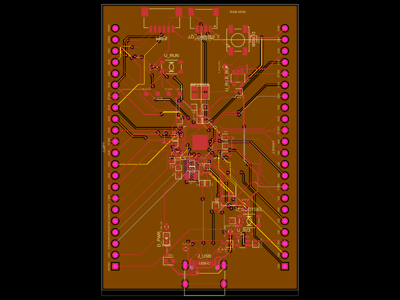 Similar packageabse/rp2350-mcu-boardThis code defines a compact, four-layer PCB hardware layout for the Raspberry Pi RP2350A microcontroller module, including the main IC, power regulation, USB-C connector, STM32-compatible headers, and associated passive components, with detailed component footprints, net connections, and copper pour zones for powering and ground references.
 Discover something newgokul/usb-hub-boardA 4-layer 100×66 mm USB 2.0 hub board with a USB‑C upstream port, four protected downstream USB‑C/USB‑A ports, an integrated SD card reader, USB hub controllers, 3.3 V regulation, ESD protection, current-limited power switches, crystal oscillators, and filtering/passive components.