abse/smartwatch-flex-top-only
Three-panel flex smartwatch with two parallel R3.9 bends, all components flat-top, low-profile JST connector harnesses, split heartbeat optical windows and screw-retained PCB mounting. Modeled 39 × 50.5 × 14.5mm prototype; 100% routing, zero native DRC and shorts. Hardware qualification pending.
- Version
- 0.2.22
- License
- unset
- Stars
- 0
qualification/requirements.json
{
  "status": "HOLD_FOR_ORDER",
  "scope": "Electrical revision of the smartwatch flex fork. Passing layout checks do not establish wireless charging, physical display-flex fit or firmware behavior.",
  "enclosureMaximumMM": {
    "width": 39,
    "length": 50.5,
    "thickness": 14.5
  },
  "display": {
    "manufacturerPartNumber": "CFAL368448A0-0193DW",
    "confirmedDrawing": {
      "bodyMaximumMM": [
        36.85,
        44.66,
        2.31
      ],
      "tailLengthNominalMM": 50,
      "tailLengthDefaultToleranceMM": 0.3,
      "tailWidthMM": 6,
      "tailWidthToleranceMM": 0.1,
      "tailThicknessMM": 0.2,
      "tailThicknessToleranceMM": 0.03,
      "contactCount": 19,
      "contactPitchMM": 0.3
    },
    "connector": "FH35C-19S-0.3SHW(50)",
    "connectorRecommendedTailWidthToleranceMM": 0.05,
    "requiredSupplierEvidence": [
      "Approve exact module/drawing identity and revision.",
      "Approve this connector's contact orientation and the tail-width tolerance difference.",
      "Provide component heights, XY keepouts and stiffener extents on both tail faces.",
      "Provide allowed bend zones, minimum radius and assembled folded-flex envelope.",
      "Provide maximum display/touch/booster start-up and steady-state current."
    ]
  },
  "fabrication": {
    "board": "4-layer flex, modeled 0.20mm; two R3.9mm static bends",
    "thermalVias": "Nine U1 EP vias per thermal-vias.json must be resin-filled and copper-capped (IPC-4761 Type VII). Ordinary tenting is insufficient.",
    "stencil": "U1 exposed land paste is reduced to 3.2x3.2mm, approximately64% area. Agree final windowing/stencil thickness with assembler; verify generated paste before release.",
    "requiredSupplierEvidence": [
      "Signed finished-copper thickness on all four layers and complete dielectric/coverlay/adhesive stack; total thickness tolerance.",
      "Approve two R3.9mm static folds, coverlay openings, six stiffeners and their adhesives.",
      "Approve filled/capped thermal via process, planarity and solderability.",
      "Solve the actual RF trace/coplanar geometry with coverlay for50ohm target; match trace width and reference-plane continuity before approving stack.",
      "Confirm placement/assembly of0201 parts and low-height connectors on the flex/stiffeners.",
      "Approve R58 dense0201 termination placement: standard0.46x0.40mm lands at0.66mm pitch with a0.10mm courtyard. Actual copper clearance and board-edge rules remain0.127/0.3mm."
    ],
    "capabilityScreen": {
      "source": "https://jlcpcb.com/capabilities/flex-pcb-capabilities",
      "checkedDate": "2026-10-13",
      "publishedFourLayerFlexThicknessOptionsMM": [
        0.2,
        0.25,
        0.3,
        0.35,
        0.4,
        0.45
      ],
      "modeledRadiusOverThickness": 19.5,
      "publishedMinimumMultilayerRadiusOverThickness": 10,
      "standardJlcProfileMatched": false,
      "viaIssue": "Current0.45/0.30mm vias have0.15mm diameter difference; JLCPCB publishes at least0.20mm difference, regular0.55/0.30mm. A qualified fabricator must approve the current annular ring/process or a separate manufacturing revision is required.",
      "clearanceIssue": "Current minimum copper clearance is0.127mm. JLCPCB publishes0.15mm exposed-pad-to-trace and coverlay-opening clearance; coverlay openings and dense package land patterns require actual DFM approval.",
      "impedanceIssue": "JLCPCB does not currently provide flex impedance measurement/control; customer must qualify the actual stack and RF geometry.",
      "scope": "Published capability screen, not a fabrication quote, supplier approval or procurement reservation. JST connector sourcing does not select the PCB fabricator."
    }
  },
  "wirelessCoil": {
    "status": "UNQUALIFIED",
    "geometry": "Existing three series-aiding6-turn spirals;0.60mm copper width,0.15mm spacing,21.6x18mm winding envelope.",
    "labelInductanceMicroH": 11,
    "labelIsMeasured": false,
    "baselineIdealDCRAt35um20COhm": 0.9378149523809528,
    "baselineQAt1MHzAssuming11uH": 73.69794883681914,
    "minimumQ": 77,
    "qualificationFrequencyHz": 1000000,
    "requiredEvidence": [
      "Measure four-wire winding DCR at recorded temperature and free-space inductance with the actual ferrite.",
      "Measure fixture inductance in final case with battery, sensor, optical hardware and ferrite.",
      "Choose C53/C54 from measured inductances; meet TI100kHz +5/-10% and1MHz +/-10% resonance windows.",
      "Calibrate FOD and measure charge current, efficiency and coil/battery/skin-side temperature on intended transmitters.",
      "Do not approve assumed11uH or a nominal copper weight as a measurement."
    ],
    "stockCoilFallback": "A qualified connector-terminated receiver-coil assembly can replace the printed winding only after a supplier drawing and a routing/assembly revision. No soldered cable splice is permitted.",
    "layoutQualification": "C73 retains the closer100nF RECT bypass; C61 is the existing RECT reservoir. Supplementary C74 is placed at(5.4,-11.2), preserving original controller exits. Measure actual RECT/OUT ripple and ringing with the final receiver layout, ferrite and load; capacitor placement and the estimated coil do not establish wireless charging qualification."
  },
  "battery": {
    "reference": "Adafruit4237 / PKcell LP552530350mAh protected reference envelope",
    "referenceMaximumContinuousDischargeA": 0.525,
    "referenceMaximumChargeA": 0.35,
    "hardwareChargeTypicalA": 0.108,
    "hardwareTerminationTypicalA": 0.003638,
    "systemCutoffTypicalV": 3.1,
    "systemCutoffRangeV": [
      3.0535,
      3.1465
    ],
    "systemRestartTypicalV": 3.3,
    "systemRestartRangeV": [
      3.2285,
      3.3715
    ],
    "requiredEvidence": [
      "Verify the already selected Adafruit4237/PKcellLP552530 pack variant, PCM limits and factory ACH crimp harness; preserve the selected body and confirm tolerance/swelling allowances.",
      "Measure battery current during radio start-up/TX, all-white display, PPG LED pulses, haptic start/stall and combinations; stay below the supplier's continuous/pulse limits.",
      "Confirm rail droop, converter efficiency and regulator/skin-side temperatures across battery voltage and temperature.",
      "Set and verify firmware load arbitration/current limits; a1A regulator does not upgrade the cell.",
      "Test charge recovery with cell below cutoff, NTC valid, open/short NTC, hot/cold NTC and MCU inhibited.",
      "Check shutdown leakage and storage behavior; the supervisor turns off the system converter and does not disconnect every battery load."
    ],
    "selectionStatus": "RETAIN_EXISTING_FORK_SELECTION",
    "manufacturerPartNumber": "LP552530",
    "supplierProductURL": "https://www.adafruit.com/product/4237",
    "selectedEnvelopeMaximumMM": [
      25.5,
      32.5,
      5.7
    ],
    "systemCutoffSenseNode": "RAW/BQ24074 OUT upstream of TPS63802",
    "systemCutoffQualification": "Threshold/restart values refer to RAW, not exact cell voltage. Battery-only cell cutoff includes actual charger power-path drop. BQ24074 specifies50mV typical/100mV maximum BAT-to-OUT dropout at1A,VIN0,VBAT>3V; selected cell permits only525mA continuous. External input regulates RAW4.3..4.5V and permits recovery/system operation. Measure cell and rail thresholds and USB/input load arbitration."
  },
  "thermistors": {
    "batteryTarget": {
      "R25Ohm": 10000,
      "resistanceTolerancePercent": 1,
      "B25_85K": 3435,
      "betaTolerancePercent": 1,
      "nominalWindowC": [
        8.08,
        41.318
      ]
    },
    "coilTarget": {
      "R25Ohm": 10000,
      "curve": "TI BQ51013B application reference NTC curve, including full R/T table; a generic10k label is insufficient."
    },
    "interface": "J7/J8 ACH2-pin, ACHR-02V-S with SACH-003G-P0.2B; compatible AWG32-30 insulated leads and factory crimped terminations, no hand-soldered splice.",
    "requiredEvidence": [
      "Exact supplier part number, R/T table, tolerances, dissipation/self-heating constant, response time and dimensioned sealed probe.",
      "Factory ACH termination compatible with the actual conductor, insulation and strain relief.",
      "Verify charging window including NTC, divider and comparator tolerances at charger-input voltage; measure self-heating and attachment lag.",
      "Probe envelope and adhesive must fit and remain attached to their intended battery/coil sensing sites."
    ],
    "selectionStatus": "RETAIN_EXISTING_10K_B3435_PROBE_SPEC_AND_ACH_HARNESS",
    "selectionEvidence": "Original electrical TH1 reference is QN0402X103F3435FA (C700819),10k B3435. Current connector assembly reuses reference sensor envelopes, with NCP03XH103F05RL named by its cover generator. These are sensor references, not proof of a stocked factory-wired ACH probe SKU."
  },
  "rfAndCrystal": {
    "rfSupplyFilter": "L5 Coilcraft0402DC-2N0XJRW2nH, C39 CL10A106KP8NNNC10uF and existing100nF C38; L5 requires assembler sourcing/consignment confirmation.",
    "crystal": "Q22FA12800332, exact JLC/LCSC C255899 catalogue binding verified:40MHz,12pF load,+/-10ppm,60ohm ESR,-40..85C. Existing18pF loads and24nH series element require oscillator start-up/frequency measurement with actual stray capacitance.",
    "requiredEvidence": [
      "Controlled-impedance stack and uninterrupted RF return plane for actual trace geometry.",
      "Enclosure/battery/ferrite/coil/connector clearance to the antenna, VNA matching and radiated RF test.",
      "Clock start-up and frequency across voltage and temperature with actual crystal, loading and PCB parasitics.",
      "Assembler approval of L5 generic0402 lands against Coilcraft recommended0.36x0.66mm pads with0.61mm inner gap; terminal width is0.47mm and current pad transverse width is0.54mm."
    ]
  },
  "firmware": "bringup-contract.json describes required behavior; no driver or firmware implementation is claimed by this PCB-only project.",
  "ordering": "No purchase or supplier message has been sent. Missing physical/supplier evidence must remain open rather than being replaced with simulated or assumed data."
}
Related Packages
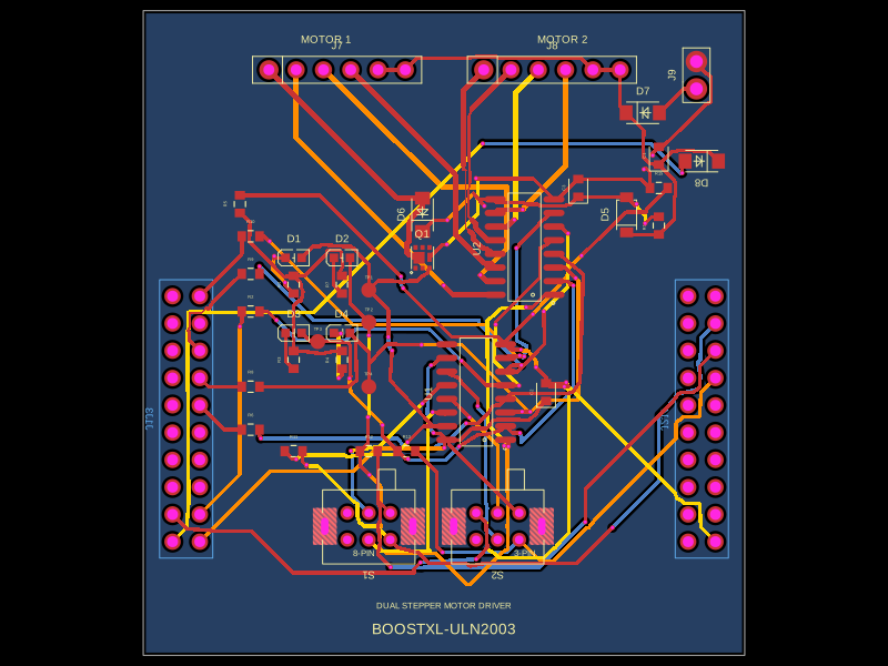 More from this authorabse/boostxl-uln2003This code defines a React component that models a through-hole or surface-mount LED with specified pin labels, footprint, silkscreen, and 3D CAD model for PCB layout.
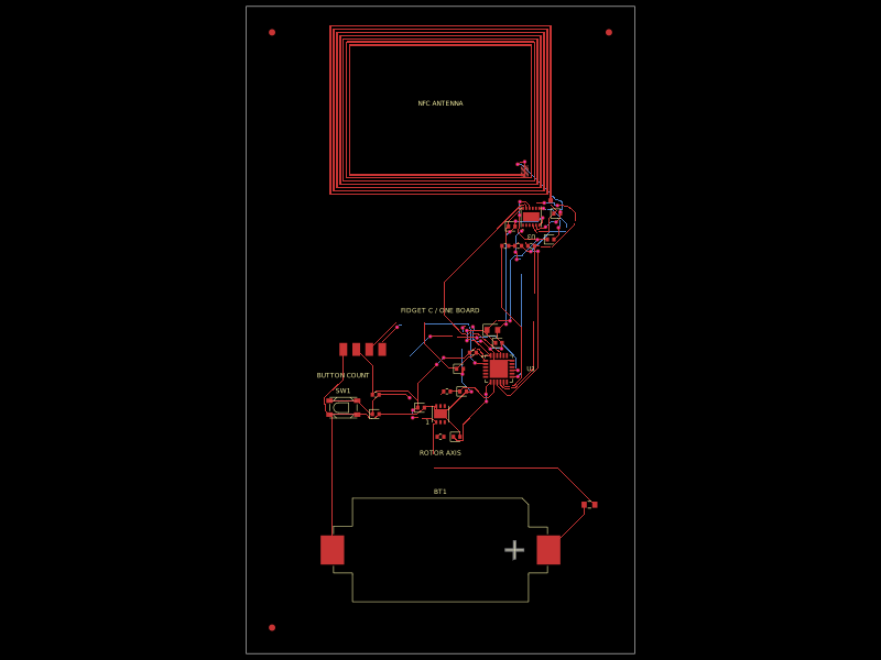 Discover something newastra/iphone-encoder-counterA CR2450-powered MSP430 FRAM counter combines an always-on dual-channel TMR rotation sensor, pushbutton input, and ST25DV NFC tag with an integrated tuned printed antenna and I²C/GPIO interface.