abse/gameboy-advance
Validates and exports a four-layer Game Boy–style PCB assembly with RP2350 MCU, 32MB flash, USB-C, LCD and speaker connectors, battery buck-boost power, buttons, and verified routing, connectivity, clearances, CAD models, and physical DRC.
- Version
- 0.0.39
- License
- unset
- Stars
- 0
PCB_FABRICATION_NOTES.txt
JLCPCB FABRICATION / ASSEMBLY NOTES

Four-layer FR-4, nominal finished thickness 1.6 mm.
USB impedance stackup: JLC04161H-3313 (JLC nominal 1.56 mm, +/-10%).
Select this stackup when ordering; do not substitute the default 7628 stackup.
L1 USB pair / L2 ground reference: target 90 ohm differential (+/-10%).
Outer copper 1 oz (0.035 mm), inner copper 0.5 oz, outer prepreg
3313: 0.0994 mm, dielectric constant 4.1, with solder mask.
Paired trunk width 0.131318 mm, edge gap 0.15 mm, coplanar ground gap
0.18 mm. Keep uninterrupted L2 ground beneath the USB paired trunks.
Geometry comes from the JLCPCB coplanar differential-pair calculator.
Have the fabricator confirm controlled impedance for its finished stackup. Use the supplied four copper
Gerbers and Edge.Cuts outline; do not replace the outline with a rectangle.
Overall bounding dimensions 144.5 x 89.55 mm include connector support tabs.
Through vias: minimum finished hole 0.30 mm, pad 0.45 mm; no blind/buried vias.
Separate plated and non-plated drill files. Four 3.3 mm mounting holes are NPTH.
Use solder mask on both sides. Do not cover test pads or connector contacts.
White silkscreen on both sides. Keep ink clear of solder-mask openings.
Added orientation/polarity text is 1 mm high. '1' identifies pin 1;
'A' identifies diode anode and 'K' identifies diode cathode.
BAT +/- identify battery terminals; SPK +/- identify driven BTL outputs.
Do not ground SPK minus. Ceramic capacitors, resistors and ordinary inductors
are nonpolar and intentionally have no +/- marks.
Populate against BOM and CPL. Review every placement rotation in JLCPCB's
assembly preview: the exporter does not certify manufacturer rotation.
Confirm MCU/QFN exposed pads, chip pin 1, diode cathodes and connector mating
orientation against manufacturer drawings before releasing assembly.
Do not substitute the LCD connector: specified 50-position 0.5 mm top-contact.
Shoulder switches have two electrical contacts and two case stakes; do not
bridge the case stakes to either signal contact during hand assembly.
External display, speaker, battery holder, batteries and enclosure hardware
are installed separately; they are not PCB assembly substitutions.
Electrical routing is unchanged by this silkscreen revision. The existing
review documents retain prototype bench qualification requirements.

Battery harness feed-through: mill the 8 x 8 mm rectangular cutout centred
at X15,Y-35 mm as drawn in Edge.Cuts. It is non-plated. Use rounded internal corners with0.5 mm router radius; do not require sharp
internal corners. Audit requires at least0.3 mm from routed traces, pads and vias to the cutout.
Measured routed clearance is0.4 mm; copper-pour clearance is0.25 mm.
JLCPCB specifies at least0.2 mm copper clearance from routed slots.
Do not replace this cutout with a 6 mm drill hole.

Revision0.0.39 uses AP63200/C2071868 and APV battery inductor/C5349662.
Logic is nominal3.234V. Populate the current BOM, including all four added
feedback/audio resistors; do not substitute the previous fixed-output regulator.
Confirm IC pin1 and polarized placements in the factory CPL preview.
Related Packages
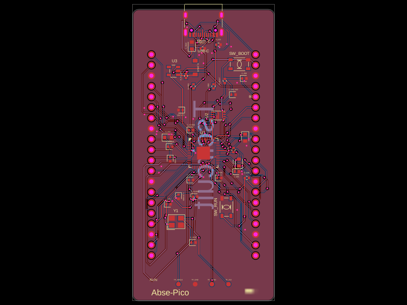 More from this authorabse/abse-picoThis code defines 3D models and footprints for various electronic components—such as voltage regulators, microcontrollers, and memory chips—highlighting their physical pin configurations, mounting pads, and visual identifiers for PCB design.
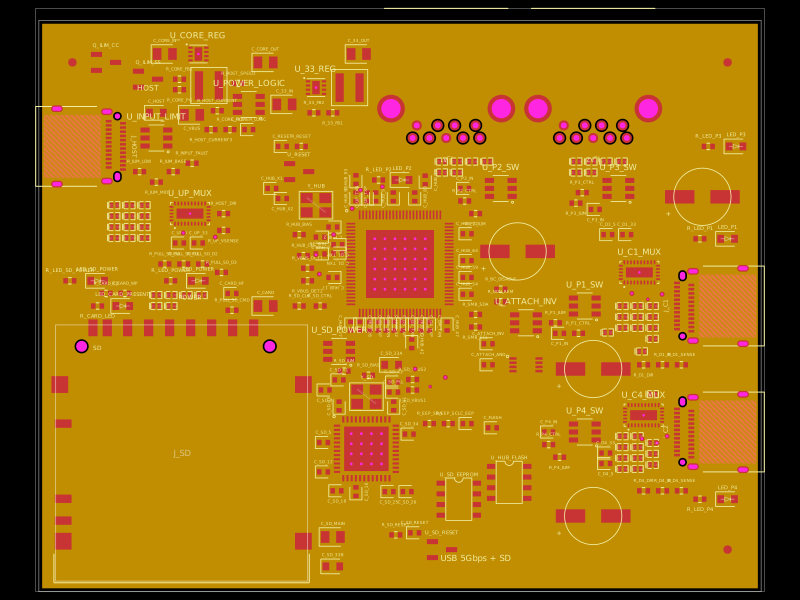 Similar packagegokul/usb3-sd-hubEngineering draft: four-layer, computer-powered USB 3 hub with one USB-C host socket, two USB-C and two USB-A accessory sockets, and a full-size SD slot. Board and three schematic previews are available. Routing and production checks are incomplete; not fabrication ready.
 Discover something newhrithik18k/smart-switch-pcbThe AO3400A component models a SOT-23 N-channel MOSFET with labeled pins for Gate, Source, and Drain, including 3D CAD models and schematic symbols for electronic circuit design.