MustafaMulla29/rp2040-bldc-motor-controller-new
A USB‑C PD–powered RP2040 BLDC motor controller PCB with 3.3 V logic, MCT8329A sensorless commutation, three MOSFET half-bridges, protected power switching, USB data, controls, and motor connectors.
- Version
- 0.3.82
- License
- unset
- Stars
- 0
scripts/pcb-audit/audit-jlcpcb.py
"""Read-only geometry/BOM preflight against selected published JLCPCB limits.
This is not JLC's own DFM review. Input and generated exports are not modified.
"""
import sys,json,math,collections,hashlib
from pathlib import Path
import geometry as R
from shapely.geometry import Point,LineString,Polygon,box
from shapely.affinity import rotate
from shapely.strtree import STRtree
P=Path(__file__).resolve().parents[2]
raw=Path(sys.argv[1]).read_bytes() if len(sys.argv)>1 else (P/'dist/index/circuit.json').read_bytes();D=json.loads(raw)
of=lambda t:[x for x in D if x['type']==t]
S={x['source_component_id']:x for x in of('source_component')};C={x['pcb_component_id']:x for x in of('pcb_component')}
SP={x['source_port_id']:x for x in of('source_port')};PP={x['pcb_port_id']:x for x in of('pcb_port')};ST={x['source_trace_id']:x for x in of('source_trace')}
NN={x['source_net_id']:x['name'] for x in of('source_net')};NK={x['subcircuit_connectivity_map_key']:x['name'] for x in of('source_net')}
xy=lambda p:(p['x'],p['y'])
LAY=['top','inner1','inner2','bottom']
def pill(x,y,w,h,ang=0):
 g=LineString([(x-max(0,w-h)/2,y-max(0,h-w)/2),(x+max(0,w-h)/2,y+max(0,h-w)/2)]).buffer(min(w,h)/2,quad_segs=48)
 return rotate(g,ang,origin=(x,y))
def padshape(p):
 if p["shape"] == "polygon": return Polygon([xy(q) for q in p["points"]])
 x,y=xy(p);k=p['shape'];ang=p.get('rect_ccw_rotation',p.get('ccw_rotation',0))
 if k=='circle':return Point(x,y).buffer(p.get('outer_diameter',p.get('radius',0)*2)/2,quad_segs=48)
 w,h=p.get('rect_pad_width',p.get('outer_width',p.get('width'))),p.get('rect_pad_height',p.get('outer_height',p.get('height')))
 if k in ['pill','rotated_pill']:return pill(x,y,w,h,ang)
 if k in ['rect','rotated_rect','rotated_pill_hole_with_rect_pad']:return rotate(box(x-w/2,y-h/2,x+w/2,y+h/2),ang,origin=(x,y))
 raise ValueError(p)
def holeshape(p):
 x,y=xy(p)
 if p.get('hole_diameter') is not None:return Point(x,y).buffer(p['hole_diameter']/2,quad_segs=48)
 return pill(x,y,p['hole_width'],p['hole_height'],p.get('hole_ccw_rotation',p.get('ccw_rotation',0)))
def padnet(p):
 s=SP[PP[p['pcb_port_id']]['source_port_id']];return NK.get(s.get('subcircuit_connectivity_map_key'),'NC_'+s['source_port_id'])
def padlabel(p):
 s=SP[PP[p['pcb_port_id']]['source_port_id']];return S[s['source_component_id']]['name']+'.'+str(s['pin_number'])
records=[];holes=[];annuli=[]
def add(kind,id,net,layers,g,label=''):
 records.append(dict(kind=kind,id=id,net=net,layers=layers,g=g,label=label))
for p in of('pcb_smtpad')+of('pcb_plated_hole'):
 kind='smd' if p['type']=='pcb_smtpad' else 'pth';id=p.get('pcb_smtpad_id',p.get('pcb_plated_hole_id'))
 g=padshape(p);net=padnet(p);label=padlabel(p);ls=p.get('layers',[p.get('layer','top')]);add(kind,id,net,ls,g,label)
 if kind=='pth':
  h=holeshape(p);holes.append(dict(kind=kind,id=id,net=net,g=h,label=label))
  ring=g.boundary.distance(h.boundary) if g.covers(h) else -1;annuli.append(dict(label=label,ring=ring))
for v in of('pcb_via'):
 net=NN.get(v.get('source_net_id')) or NK.get(v.get('subcircuit_connectivity_map_key'));assert net
 add('via',v['pcb_via_id'],net,v['layers'],Point(*xy(v)).buffer(v['outer_diameter']/2,quad_segs=48))
 holes.append(dict(kind='via',id=v['pcb_via_id'],net=net,g=holeshape(v),label=v['pcb_via_id']))
for t in of('pcb_trace'):
 net=NN.get(t.get('connection_name')) or NK.get(ST.get(t.get('source_trace_id'),{}).get('subcircuit_connectivity_map_key'));assert net
 for a,b in zip(t['route'],t['route'][1:]):
  if a['route_type']==b['route_type']=='wire' and a['layer']==b['layer'] and math.dist(xy(a),xy(b))>1e-9:
   add('trace',t['pcb_trace_id'],net,[a['layer']],LineString([xy(a),xy(b)]).buffer(a['width']/2,quad_segs=32))
for p in of('pcb_copper_pour'):
 assert p['shape']=='brep';b=p['brep_shape'];g=Polygon([xy(v) for v in b['outer_ring']['vertices']],[[xy(v) for v in r['vertices']] for r in b.get('inner_rings',[])])
 add('pour',p['pcb_copper_pour_id'],NN[p['source_net_id']],[p['layer']],g)
checks=collections.defaultdict(dict)
def hit(rule,key,data):
 old=checks[rule].get(key)
 if old is None or data['gap']<old['gap']:checks[rule][key]=data
# Hole to unrelated trace/copper: use separate published inner-layer rules.
for l in LAY:
 rs=[r for r in records if l in r['layers']];tree=STRtree([r['g'] for r in rs])
 for h in holes:
  for i in tree.query(h['g'].buffer(.301)):
   r=rs[int(i)]
   if h['net']==r['net']:continue
   if l.startswith('inner'):limit=.2 if h['kind']=='via' else .3;rule=h['kind']+'_hole_to_inner_copper'
   elif r['kind']=='trace':limit=.2 if h['kind']=='via' else .28;rule=h['kind']+'_hole_to_outer_trace'
   else:continue
   gap=h['g'].distance(r['g'])
   if gap<limit-1e-5:hit(rule,(h['id'],r['id'],l),dict(hole=h['label'],hole_net=h['net'],other=r['label'] or r['id'],other_net=r['net'],layer=l,gap=gap,required=limit,location=list(h['g'].centroid.coords)[0]))
 # Test all foreign copper pairs as well as drill and footprint rules.
 for i,a in enumerate(rs):
  for jj in tree.query(a['g'].buffer(.10001)):
   j=int(jj);b=rs[j]
   if j<=i or a['net']==b['net']:continue
   gap=a['g'].distance(b['g'])
   if gap<.1-1e-5:hit('foreign_copper_gap',(a['id'],b['id'],l),dict(a=a['label'] or a['id'],a_net=a['net'],b=b['label'] or b['id'],b_net=b['net'],gap=gap,required=.1,layer=l))
 sm=[r for r in rs if r['kind']=='smd'];stree=STRtree([r['g'] for r in sm])
 for i,a in enumerate(sm):
  for j in stree.query(a['g'].buffer(.151)):
   j=int(j);b=sm[j]
   if j<=i or a['net']==b['net']:continue
   gap=a['g'].distance(b['g'])
   if gap<.15-1e-5:hit('smd_pad_gap',(a['id'],b['id']),dict(a=a['label'],b=b['label'],gap=gap,required=.15,layer=l))
htree=STRtree([h['g'] for h in holes])
for i,a in enumerate(holes):
 for j in htree.query(a['g'].buffer(.451)):
  j=int(j);b=holes[j]
  if j<=i:continue
  if a['kind']==b['kind']=='via':lim=.2;rule='via_hole_to_hole'
  elif a['kind']==b['kind']=='pth':lim=.45;rule='pth_hole_to_hole'
  else:continue # Mixed hole class is not expressly resolved by the published table.
  gap=a['g'].distance(b['g'])
  if gap<lim-1e-5:hit(rule,(a['id'],b['id']),dict(a=a['label'],b=b['label'],gap=gap,required=lim))
board=of('pcb_board')[0]
if board.get('outline'):
 outline=Polygon([xy(p) for p in board['outline']])
else:
 center=board.get('center',{'x':0,'y':0})
 outline=box(center['x']-board['width']/2,center['y']-board['height']/2,center['x']+board['width']/2,center['y']+board['height']/2)
for r in records:
 gap=outline.boundary.distance(r['g']) if outline.covers(r['g']) else -1
 if gap<.2-1e-5:hit('copper_edge',(r['id'],),dict(id=r['label'] or r['id'],net=r['net'],gap=gap,required=.2))
# Native pad testpoints are fabricated copper, not purchased assembly parts.
fitted=[s for s in S.values() if not (s['ftype']=='simple_test_point' and s.get('footprint_variant')=='pad')]
missing=[dict(name=s['name'],type=s['ftype']) for s in fitted if not s.get('manufacturer_part_number')]
smalltext=[dict(text=t['text'],font_size=t['font_size'],layer=t['layer']) for t in of('pcb_silkscreen_text') if t.get('font_size',2)<1]
O=dict(sha256=hashlib.sha256(raw).hexdigest(),real_components=len(fitted),native_testpads=len(S)-len(fitted),missing_mpn=missing,small_silkscreen_text=smalltext,pth_annuli=annuli,findings={k:sorted(v.values(),key=lambda x:x['gap']) for k,v in checks.items()})
out=R.BASE/'jlcpcb-preflight.json';out.write_text(json.dumps(O,indent=2)+'\n')
print('SHA',O['sha256'],'missing parts',len(missing),'small silkscreen text',len(smalltext),'min PTH ring',min(x['ring'] for x in annuli))
for k,v in O['findings'].items():print(k,len(v),json.dumps(v[:4]))
Related Packages
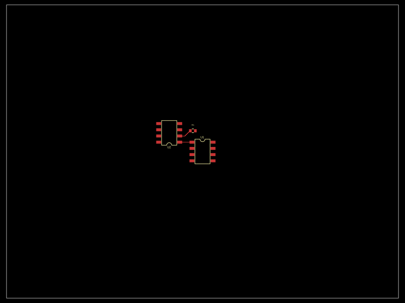 More from this authorMustafaMulla29/auto-placeA small PCB featuring two SOIC-8 ICs interconnected with a resistor.
 Similar packageimrishabh18/rp2040-motor-controllerAn RP2040-based NEMA17 stepper-motor controller with USB-C programming and PD motor-power negotiation, DRV8825 dual H-bridge drive, current/temperature telemetry, protected power filtering, status RGB LED, buzzer alarm, and optional magnetic encoder.
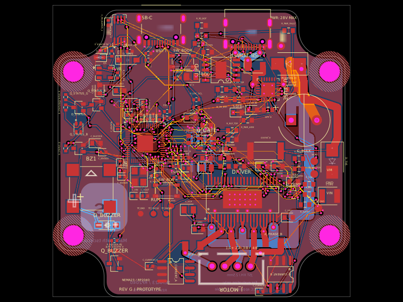 Discover something newimrishabh18/nema-23-stepper-controllerA curved NEMA23 rear-mount PCB combining an RP2040 controller, USB-C/USB-PD power input and protection, DRV8452 dual-winding stepper driver, current sensing, thermal interlock, status RGB LED, buzzer, and optional I²C encoder interface.