MustafaMulla29/rp2040-bldc-motor-controller-new
A USB‑C PD–powered RP2040 BLDC motor controller PCB with 3.3 V logic, MCT8329A sensorless commutation, three MOSFET half-bridges, protected power switching, USB data, controls, and motor connectors.
- Version
- 0.3.82
- License
- unset
- Stars
- 0
manufacturing/assembly-instructions.md
# Factory review instructions

Design: rp2040-bldc-motor-controller-new, 73 × 72 mm, four layers.
Status: 12 October 2026 engineering review only. Hold fabrication/assembly pending the U7 stencil and remaining release findings in `order-readiness.md`. Production approval has not been obtained.

## PCB fabrication

Use JLC04161H-3313, nominal 1.6 mm thickness, 1 oz outer copper and 0.5 oz inner copper. The construction and USB requirements are in `stackup.json`. Preserve the finished 73 × 72 mm outline. Add panel rails, tooling and panel fiducials externally as needed for assembly; do not place them over the circuit. Every via is 0.30 mm drill / 0.45 mm pad. Do not change copper weight or substitute a thicker L1–L2 dielectric without another USB calculation and clearance review.

The L1 USB data routes reference the L2 GND plane. Target 90 Ω differential, ±15%. Main traces are 0.15 mm wide; the two short connector reversal links are 0.125 mm. Spacing varies through the connector, ESD array and resistor fanouts. Please calculate using the actual supplied geometry and identify any required width changes before fabrication. Do not assume a uniform coupled pair or certify the complete channel from a coupon alone.

## Assembly scope and placement

Fit **all 155 BOM components**, all mounted on the top side; verify the newly generated assembly-scope.csv. Use `bom.csv`, `cpl-reviewed.csv` and `assembly-scope.csv` from `dist/assembly-review`. The latter identifies the mounting process and side for each part. The separate native CLI export may contain an unreviewed fallback CPL; do not use that file instead.

The reviewed CPL uses millimeters in the same board coordinate system as the Gerbers. The board is centered at (-3.5, 9.5) mm, with X bounds -40 to 33 mm and Y bounds -26.5 to 45.5 mm; negative coordinates are intentional. Rotation is the numbered supplier footprint's orientation, all placed from the top side. Confirm the factory library's convention in its placement preview before production.

J1 and J19 are HRO TYPE-C-31-M-12, C165948. Their corrected land patterns have asymmetric copper bounds, so the CPL coordinates use the supplier datum registered to the four shell-slot centers. Check their shell slots and plastic pegs together in the preview; do not recenter on the copper bounds. Both mouths face the left board edge. J1 is DATA; J19 is USB PD.

Factory solder all **five through-hole components**:

| Side | Components |
| --- | --- |
| Top | C93, J10, J11, J12, RV1 |

Also solder the retention tabs of J1 and J19. Use the suitable selective/manual soldering process and fixtures for top-inserted THT parts; these parts must not be left for the customer to solder. Confirm the mixed assembly process and fixture requirements in the quote.

J10/J11/J12: AMASS 24.243.4 (C7437324), top-mounted, opening toward the top board edge; U/V/W respectively. Both solder legs of each socket are the same phase. Three purchased BDHI B117-5 rigid adapters are offboard accessories; no custom motor wire harness is specified. Check IC pin 1, diode/LED cathodes and C93 positive lead against the numbered pad review and assembly drawing. C93 is top-side and 16 mm tall. SW1–SW4 and RV1 are operated directly onboard. TP1–TP16 are unpopulated copper pads: no assembly parts and no paste. Allow space below for through-hole solder tails and mounting hardware; there are no bottom component bodies.

SW4 is C&K JS202011JCQN (C221665), top-actuated SMT DPDT. Retain the corrected 2.50 mm contact pitch from the C&K I-56 drawing (the imported library used 2.54 mm). At its 90° board rotation, OFF is toward −Y and ON toward +Y. Verify contact operation against the OFF/ON silkscreen before release. U11 is TPS1H100AQPWPRQ1 (C478465); its pin-15 ground pad is 2.60 × 2.59 mm per TI PWP0014K. D6 cathode faces the reverse-isolated PD_LOAD net, and D7 cathode is the POWER_ON_LEVEL clamp.

## Production stencil

Use the U7 exposed-pad instruction in `stencil-u7.svg` and `stencil-u7.json`: six rounded rectangular apertures, 1.05 × 1.15 mm, R0.05, centers X = −1.20/0/+1.20 mm and Y = −0.65/+0.65 mm relative to pad 37. This yields approximately 74.8% coverage on the authored 3.650 × 2.650 mm pad. Start from a 0.125 mm stencil, following TI's REE0036A example, and confirm release/coverage with the stencil engineer.

**The native F_Paste export now has six 1.05 × 1.15 mm rectangular U7 exposed-pad windows (74.90% area), with the original central paste opening suppressed. Their positions and sizes are checked against the drawing. Native `<solderpaste>` does not support rounded corners yet: the R0.05 rounding in the factory instruction (~74.77% area) remains a stencil-engineering request, not exported geometry.** Please provide the production stencil drawing for approval. Review other QFN exposed pads and small-component apertures under the same process. Omit paste from ordinary THT pads; solder those in the separate THT process. The native B_Paste file contains 8 USB shell-slot flashes and must not be treated as a request for bottom SMT assembly or THT paste. Do not introduce pin-in-paste processing without review.

U11: follow TI PWP0014K drawing 4229706/B. The authored exposed copper pad is 2.60 × 2.59 mm in component axes (2.59 × 2.60 mm in board axes). **The native paste opening is now 2.590 × 2.600 mm in board axes, matching TI's 2.60 × 2.59 mm example for a 0.125 mm stencil.** The source footprint uses `solderPasteMargin={0}` and the export is checked by `check-native-stencil.mjs`. Approve solder release and final coverage with the stencil engineer. The eight nearby thermal vias are outside this solder land. If stencil thickness changes, review TI’s corresponding opening dimensions rather than scaling all apertures blindly. U1 and U5 exposed pads also export as single rectangles at approximately 49% area and require process review. Paste area is not itself a final solder-coverage measurement.

JLCPCB prepares the production stencil from its verified SMT assembly data and accepts custom stencil requirements in the order remarks. These files supply that requirement; they do not claim it has already been implemented or approved by the factory. See [JLCPCB's stencil preparation process](https://jlcpcb.com/help/article/smt-stencil-data-prepared-for-smt-orders) and [TI's REE0036A stencil example](https://www.ti.com/lit/ds/symlink/mct8329a.pdf#page=163).

## Before approving production

Resolve the layout/release hold in `order-readiness.md` first. Confirm part stock and any substitutions against the exact BOM, inspect the factory top-side placement preview and THT tail clearance, approve the U7/U11 stencil drawings and USB geometry calculation, and verify that the quote includes all THT soldering. This is an unprogrammed prototype: STUSB4500 default-9 V provisioning, runtime 5/9/15/20 V verification and motor firmware are separate from PCB assembly.

The USB power/data cables and purchased motor adapters are offboard accessories, specified in `docs/offboard-parts.csv`. There is no battery or temperature-probe wiring. Speed, ARM and POWER controls are onboard.

Process references: [JLCPCB mixed/THT assembly capability](https://jlcpcb.com/capabilities/pcb-assembly-capabilities), [fixtures for assembly, including THT on both faces](https://jlcpcb.com/help/article/pcb-assembly-fixtures), [layer constructions](https://jlcpcb.com/impedance).

RV1 is Alps RK09K1130A8G / C470294. Its corrected mounting pattern follows Alps Drawing 2, including 8.8 mm tab spacing and 1.8 × 2.1 mm mounting slots. Do not substitute the supplier library's original 10 mm tab spacing. Review the registered model and mounting-tab datum. SW1–SW3 use TS-1187A-B-A-B / C318884.

Configurable-PD trial: R142 is 1.5 kΩ (C22843), setting approximately 1.64 A nominal motor-feed current limiting. F1 and U12/Q7 are the fused, reverse-isolated motor feed. Q1/Q2 are SI4427BDY-T1-E3, D1 is BZT52C8V2, D4 is SMBJ22A, bridge MOSFETs are AOD2610E, and C93 is Panasonic EEUFR1H471 (12.5 x 20 mm). Check exact part references against the regenerated BOM; removed battery/charger components are not fitted.

## Q7 PowerDI3333 stencil (trial)

Q7 retains the continuous catalog drain-copper polygon. Eight native rectangular paste apertures replace its automatic polygon opening: four 1.05 × 0.70 mm windows over the exposed pad and four 0.35 × 0.49 mm drain-finger apertures. Copper is unchanged. The Gerber checker verifies all eight native flashes. Approve stencil thickness, release, corner rounding and voiding with the factory; this is an authored trial pattern, not a manufacturer-approved stencil. At 0.125 mm thickness the smallest aperture has an area ratio of about 0.817.

The Q7 CPL uses the catalog numbered-pad datum rather than its asymmetric copper-bounds center. AOD2610E uses the reviewed larger TO-252 lands; each contains the corresponding catalog land at the authored body datum. The tab is electrical drain pin 2 (catalog labels it 4). Check the supplier's actual library placement preview.
Related Packages
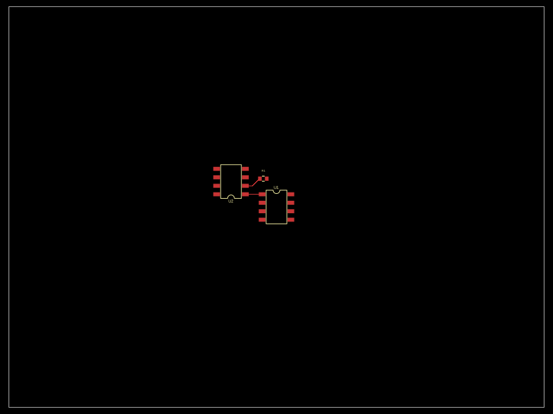 More from this authorMustafaMulla29/auto-placeA small PCB featuring two SOIC-8 ICs interconnected with a resistor.
 Similar packageimrishabh18/rp2040-motor-controllerAn RP2040-based NEMA17 stepper-motor controller with USB-C programming and PD motor-power negotiation, DRV8825 dual H-bridge drive, current/temperature telemetry, protected power filtering, status RGB LED, buzzer alarm, and optional magnetic encoder.
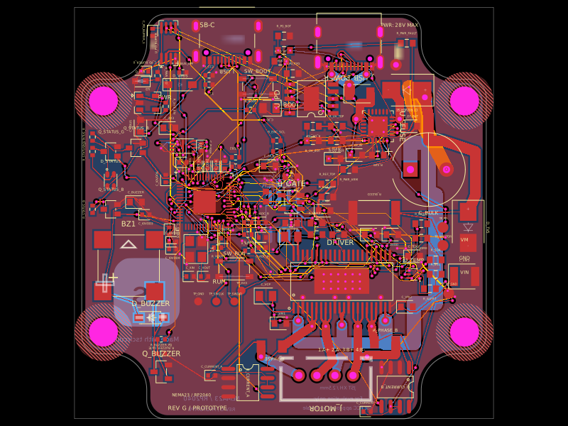 Discover something newimrishabh18/nema-23-stepper-controllerA curved NEMA23 rear-mount PCB combining an RP2040 controller, USB-C/USB-PD power input and protection, DRV8452 dual-winding stepper driver, current sensing, thermal interlock, status RGB LED, buzzer, and optional I²C encoder interface.