MustafaMulla29/rp2040-bldc-motor-controller-new
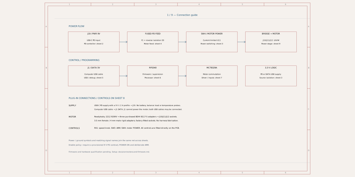
A 9V USB‑PD RP2040 controller board with MCT8329A sensorless BLDC driver, three MOSFET half-bridges, protected power switching, USB data/programming, and onboard speed/arm controls for a three-phase motor.
- Version
- 0.3.81
- License
- unset
- Stars
- 0
index.circuit.tsx
PCB
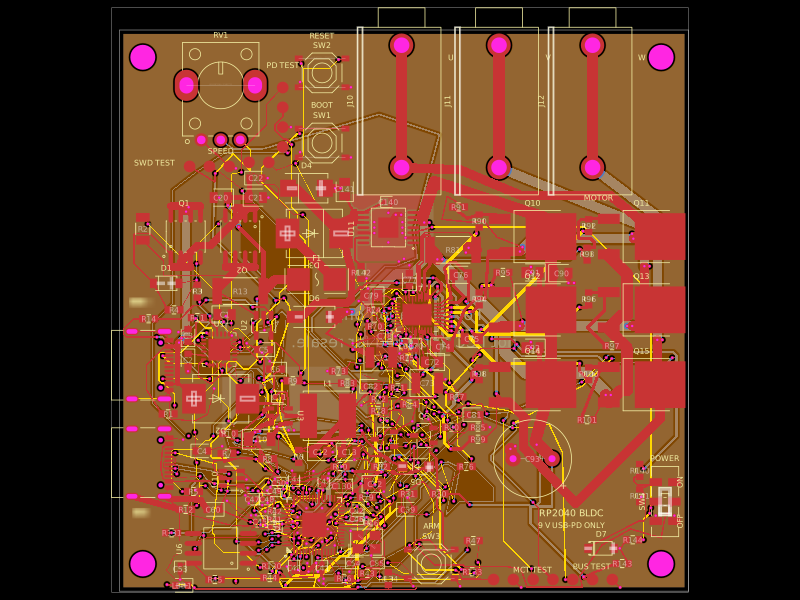
Schematic
import kelvinPours from "./circuit/kelvin-pour-outlines.json"
import { PowerSwitch } from "./circuit/power-switch"
import { AssemblyReferences } from "./circuit/assembly-references"
import { savedRouting } from "./circuit/saved-routing"
import { UsbPd, LogicPower } from "./circuit/power"
import { SeparateUsb } from "./circuit/usb-ports"
import { PdLoad } from "./circuit/pd-load"
import { Processor } from "./circuit/processor"
import { MotorControl, MotorBridge } from "./circuit/motor"
import type { BoardProps } from "@tscircuit/props"
import { Fragment } from "react"
import { RoutingPlan } from "./circuit/routing-plan"
import { SchematicNotes } from "./circuit/schematic-notes"

/** 9 V USB-PD motor supply, no battery, RP2040 USB data.
 * Saved routing is tied to the exact pad, net and rule input.
 * Engineering prototype; power integrity and fault behaviour need bench validation.
 */
export default function PicoPdMotorLab({ routingAlgorithm = savedRouting, ...props }:
  Partial<BoardProps> & { routingAlgorithm?: typeof savedRouting } = {}) {
  return <board width={73} height={72} outlineOffsetX={-3.5} outlineOffsetY={9.5} layers={4} thickness="1.6mm"
    autorouter={{ local: true, algorithmFn: routingAlgorithm }} autorouterVersion="latest" autorouterEffortLevel="1x"
    routeRemaining
    minTraceWidth={0.1} minTraceToPadEdgeClearance={0.1}
    minViaEdgeToPadEdgeClearance={0.1} minViaHoleEdgeToViaHoleEdgeClearance={0.3}
    minViaHoleDiameter="0.3mm" minViaPadDiameter="0.45mm"
    pcbStyle={{ viaHoleDiameter: "0.3mm", viaPadDiameter: "0.45mm" }}
    isViaInPadAllowed={false} allowBlindAndBuriedVias={false}
    schTraceAutoLabelEnabled schMaxTraceDistance={12} {...props}>
    <RoutingPlan />
    <group name="pcb_power_switch" pcbX={0} pcbY={0} schX={0} schY={0}><PowerSwitch /></group>
    <AssemblyReferences />
    {/* Standard through-vias outside solder lands; 0.30 mm drill / 0.45 mm pad. */}
    {[
      [-17.15,-19],[-17.15,-17],[-12.85,-19],[-12.85,-17],
      [-16,-20.4],[-14,-20.15],[-16,-15.85],[-14,-15.85],
      [-4.15,15.8],[-3.5,16.15],[-2.65,6.125],[-4.6,6.2],
      [-18.3,-5.85],[-17.6,-5.85],
    ].map(([x,y],i) => <Fragment key={i}><via name={`GND_STITCH_${i+1}`} pcbX={x} pcbY={y}
      fromLayer="top" toLayer="bottom" layers={["top","inner1","inner2","bottom"]}
      holeDiameter="0.3mm" outerDiameter="0.45mm" tented connectsTo="net.GND" /></Fragment>)}
    {/* U11 thermal pad: copper on both faces and eight through-vias outside the solder land. */}
    {[[-.7,-1.8],[0,-1.8],[.7,-1.8],[-.7,1.8],[0,1.8],[.7,1.8],[-1.9,0],[1.9,0]].map(([x,y],i) =>
      <Fragment key={`power-${i}`}><via name={`POWER_GND_${i+1}`} pcbX={-5.5-y} pcbY={20.15+x}
        fromLayer="top" toLayer="bottom" layers={["top","inner1","inner2","bottom"]}
        holeDiameter="0.3mm" outerDiameter="0.45mm" tented connectsTo="net.GND" /></Fragment>)}
    {/* Top pours stop 0.2 mm from the isolated SN copper. L2 stays continuous. */}
    {kelvinPours.powerTop.map((outline,i) => <Fragment key={`power-top-${i}`}><copperpour name={`POWER_GROUND_top_${i}`}
      connectsTo="net.GND" layer="top" clearance={0.2} useThermalReliefs={false} outline={outline} /></Fragment>)}
    <copperpour name="POWER_GROUND_bottom" connectsTo="net.GND" layer="bottom" clearance={0.2} useThermalReliefs={false}
      outline={[{x:-10.5,y:15.65},{x:0.5,y:15.65},{x:0.5,y:24.65},{x:-10.5,y:24.65}]} />
    <SchematicNotes />
    <copperpour name="GROUND_BOTTOM" connectsTo="net.GND" layer="bottom" clearance={0.25} boardEdgeMargin={0.5} useThermalReliefs={false} />
    <copperpour name="GROUND_PLANE" connectsTo="net.GND" layer="inner1" unbroken clearance={0.2} boardEdgeMargin={0.5} useThermalReliefs={false} />
    {/* Local ground copper spreads driver heat and closes bypass loops. */}
    {kelvinPours.motorTop.map((outline,i) => <Fragment key={`motor-top-${i}`}><copperpour name={`MOTOR_GROUND_TOP_${i}`}
      connectsTo="net.GND" layer="top" clearance={0.2} useThermalReliefs={false} outline={outline} /></Fragment>)}
    <copperpour name="MOTOR_GROUND_BOTTOM" connectsTo="net.GND" layer="bottom" clearance={0.2} useThermalReliefs={false}
      outline={[{x:-8.8,y:2.5},{x:1.5,y:2.5},{x:1.5,y:15.8},{x:-8.8,y:15.8}]} />
    <copperpour name="LOGIC_GROUND_BOTTOM" connectsTo="net.GND" layer="bottom" clearance={0.2} useThermalReliefs={false}
      outline={[{x:-27,y:-7},{x:-8,y:-7},{x:-8,y:2.5},{x:-27,y:2.5}]} />
    <copperpour name="PROCESSOR_GROUND_TOP" connectsTo="net.GND" layer="top" clearance={0.2} useThermalReliefs={false}
      outline={[{x:-19.1,y:-22.3},{x:-10.9,y:-22.3},{x:-10.9,y:-13.9},{x:-19.1,y:-13.9}]} />
    <group pcbX={0} pcbY={0} schX={0} schY={0} name="pcb_usb_pd"><UsbPd /></group>
    <group pcbX={0} pcbY={0} schX={0} schY={0} name="pcb_logic_power"><LogicPower /></group>
    <group pcbX={0} pcbY={0} schX={0} schY={0} name="pcb_pd_load"><PdLoad /></group>
    <group pcbX={0} pcbY={0} schX={0} schY={0} name="pcb_processor"><Processor /></group>
    <group pcbX={0} pcbY={0} schX={0} schY={0} name="pcb_motor_control"><MotorControl /></group>
    <group pcbX={0} pcbY={0} schX={0} schY={0} name="pcb_bridge"><MotorBridge /></group>
    <group pcbX={0} pcbY={0} schX={0} schY={0} name="pcb_separate_usb"><SeparateUsb /></group>
    {[[-37,-23],[29.5,-23],[-37,42],[29.5,42]].map(([x,y], i) =>
      <Fragment key={i}><hole name={`H${i+1}`} diameter={3.2} pcbX={x} pcbY={y} /></Fragment>)}
    <silkscreentext text="POWER" pcbX={30} pcbY={-9.4} fontSize={1} />
    <silkscreentext text="OFF" pcbX={31.9} pcbY={-17.5} pcbRotation={90} fontSize={1} />
    <silkscreentext text="ON" pcbX={31.9} pcbY={-12.5} pcbRotation={90} fontSize={1} />
    <silkscreentext text="RP2040 BLDC" pcbX={18} pcbY={-16.5} fontSize={1.2} />
    <silkscreentext text="9 V USB-PD ONLY" pcbX={18} pcbY={-18} fontSize={1} />
    {/* Back-side evaluation notice, shared by the PCB and integrated assembly entrypoints. */}
    <silkscreentext text="For evaluation only;" layer="bottom" pcbX={-3.5} pcbY={9} fontSize={2} />
    <silkscreentext text="not FCC approved for resale." layer="bottom" pcbX={-3.5} pcbY={5.5} fontSize={2} />
    {/* tscircuit2024 has no semicolon glyph: native artwork completes its reserved character cell. */}
    <silkscreenpath layer="bottom" strokeWidth={0.18} route={[{x:-16.38,y:9.15},{x:-16.50,y:9.15}]} />
    <silkscreenpath layer="bottom" strokeWidth={0.18} route={[{x:-16.50,y:8.53},{x:-16.30,y:8.28}]} />
    <silkscreentext text="MOTOR" pcbX={21.5} pcbY={24} fontSize={1} />
    <silkscreentext text="DATA" pcbX={-36.5} pcbY={-16.5} fontSize={1.2} isKnockout knockoutPadding={0.25} />
    <silkscreentext text="PD 9V" pcbX={-36.5} pcbY={10.5} fontSize={1.2} isKnockout knockoutPadding={0.25} />
    {[-3.8,8.7,20.7].map((x,i) => <Fragment key={i}><silkscreentext text={"UVW"[i]} pcbX={x+6.35} pcbY={42} fontSize={1} /></Fragment>)}
    {[
      ["SWD TEST",-35.5,28.5], ["RESET",-14,44.8],
      ["ARM",0,-18.1], ["BOOT",-14,35.9], ["PD TEST",-19,41],
       ["MCT TEST",13,-23.7], ["SPEED",-27,30],
      ["BUS TEST",20.6,-23.3],
    ].map(([label,x,y],i) => <Fragment key={i}><silkscreentext text={String(label)} pcbX={Number(x)} pcbY={Number(y)} fontSize={1} /></Fragment>)}
    {/* Local VREG bypass connectivity; the saved plan contains its short physical path. */}
    <trace name="MCT_REGULATOR_BYPASS" from=".U7 > .VREG" to=".C80 > .pin1" thickness={0.2} />
  </board>
}