MustafaMulla29/rp2040-bldc-motor-controller-new
A USB‑C PD–powered RP2040 BLDC motor controller PCB with 3.3 V logic, MCT8329A sensorless commutation, three MOSFET half-bridges, protected power switching, USB data, controls, and motor connectors.
- Version
- 0.3.82
- License
- unset
- Stars
- 0
docs/usb-footprint-review.md
# USB-C connector drawing check

J1 (DATA) and J19 (PWR 9V) use the **HRO TYPE-C-31-M-12**, LCSC **C165948**. USB-C describes the mating interface; PCB mounting footprints differ between connector models. Do not substitute another receptacle without comparing its drawing.

J1 and J19 are declared directly as native `<connector standard="usb_c" manufacturerPartNumber="TYPE-C-31-M-12">` elements. Their symbols use tscircuit's default USB-C pin arrangement and automatic dimensions. `circuit/usb-c-footprint.tsx` holds the manufacturer-checked land pattern, physical pin aliases and CAD model. The original JLCPCB import wrapper and the manual schematic pin-arrangement overrides have been removed. Numeric pad IDs remain mapped to the manufacturer's physical contacts below.

Checked against the [HRO drawing, dated 2020-12-08](https://datasheet.lcsc.com/datasheet/pdf/9e56b777c022540fcce7c7f67825f55e.pdf?productCode=C165948), component-side recommended PCB layout:

| Feature | Authored geometry |
|---|---|
| Eight signal lands | 0.30 mm wide, 0.50 mm pitch |
| Four combined VBUS/GND lands | 0.60 mm wide, at x = ±2.40 / ±3.20 mm |
| Land length | 1.14 mm: drawing's 1.64 mm minus 0.50 mm datum offsets |
| Land row | Lower edge aligned with the rear shell-slot centre line |
| Shell slots | 0.60 mm drill width; 0.90 mm copper width |
| Rear shell slots | 1.70 mm drill length; 2.00 mm copper length |
| Front shell slots | 1.40 mm drill length; 1.70 mm copper length |
| Shell centres | 8.65 mm horizontal pitch, 4.18 mm row spacing |
| Plastic locating pegs | Two 0.60 mm NPTH, 5.78 mm pitch |
| Board edge | 5.79 mm in front of the rear shell-slot centre line |

The previous library footprint had wider mounting slots and an offset, longer signal-pad row. Those dimensions were corrected; both sockets were repositioned to put the drawing's PCB-edge datum on the left edge of the board. The connector housing deliberately projects beyond that edge.

| Source pad ID | HRO contact | Function |
|---|---|---|
| 1–4 | Shell retention tabs | Shield, connected to GND |
| 5 | B8 | SBU2, unused |
| 6 | A5 | CC1 |
| 7 | B7 | D−, orientation 2 |
| 8 | A6 | D+, orientation 1 |
| 9 | A7 | D−, orientation 1 |
| 10 | B6 | D+, orientation 2 |
| 11 | A8 | SBU1, unused |
| 12 | B5 | CC2 |
| 13 | A1/B12 | GND |
| 14 | B1/A12 | GND |
| 15 | B4/A9 | VBUS |
| 16 | A4/B9 | VBUS |

On J1, the two D+ contacts share USB_DP, and the two D− contacts share USB_DM. CC1 and CC2 each have their own 5.1 kΩ pull-down. On J19, CC1/CC2 go to the STUSB4500; data contacts are unused. The two VBUS domains remain separate.

This is a drawing and CAD comparison. Physical fit, soldering and USB operation still require inspection of the first assembly.
Related Packages
 More from this authorMustafaMulla29/auto-placeA small PCB featuring two SOIC-8 ICs interconnected with a resistor.
 Similar packageimrishabh18/rp2040-motor-controllerAn RP2040-based NEMA17 stepper-motor controller with USB-C programming and PD motor-power negotiation, DRV8825 dual H-bridge drive, current/temperature telemetry, protected power filtering, status RGB LED, buzzer alarm, and optional magnetic encoder.
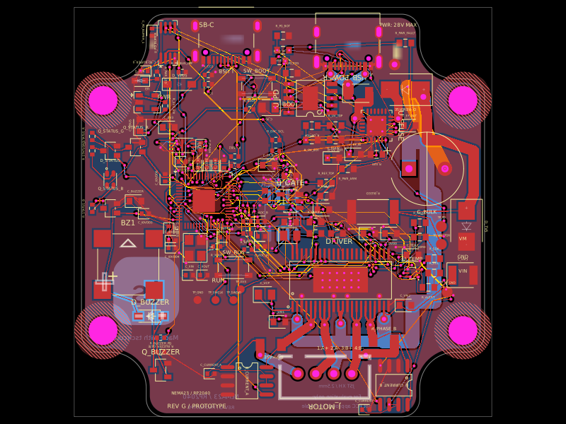 Discover something newimrishabh18/nema-23-stepper-controllerA curved NEMA23 rear-mount PCB combining an RP2040 controller, USB-C/USB-PD power input and protection, DRV8452 dual-winding stepper driver, current sensing, thermal interlock, status RGB LED, buzzer, and optional I²C encoder interface.