MustafaMulla29/rp2040-bldc-motor-controller-new
A USB‑C PD–powered RP2040 BLDC motor controller PCB with 3.3 V logic, MCT8329A sensorless commutation, three MOSFET half-bridges, protected power switching, USB data, controls, and motor connectors.
- Version
- 0.3.82
- License
- unset
- Stars
- 0
docs/routing.md
# Routing validation

`circuit/route-plan.json` contains authored copper, guarded by the exact current placement/net/rule input. Unchanged verified copper is retained; changed supply and interlock nets are rerouted. Deleted component branches are removed. Generated circuit JSON and error records are never modified.

The current compact outline is 73 × 72 mm; see the sixth review below. The power-layout review changed 47 component positions or orientations before the subsequent compacting passes. Input FETs, the shunt, fuse, protection diode and power switch IC are grouped together; gate resistors, bootstrap capacitors and the bridge shunt are placed around the motor driver and bridge. Native placement checking reports no placement issues and zero placement DRC errors/warnings. Component courtyards and 6.4 mm mounting-screw envelopes do not overlap. The later [order-readiness review](order-readiness.md) identified a current-sense routing problem. The Kelvin revision below corrects it and adds a dedicated regression check.

Main 9 V input and motor-current routes now use top/bottom copper. Inner1 remains the uninterrupted GND reference, with additional bottom GND copper; signal and gate-drive routing can still use inner2. Gate runs are 0.4 mm with short 0.18–0.22 mm fine-pitch pin escapes. Vias use 0.30 mm drills and 0.45 mm pads; motor-current transitions retain parallel pairs with common broad copper. All components remain on top, and the minimum signal width remains 0.10 mm.

The initial routing revision decreased unique vias from 756 to 491. The follow-up cleanup removes 32 unnecessary single-layer vias and trims their unused trace tails. All 3.3 V supply branches now have at least 0.2 mm copper width, with local rerouting to retain clearance. BOOT, RESET and ARM text is separated from the switch references. The GLA net's routed copper length decreases from 108.08 mm to 26.05 mm, and its via count from 12 to 3. The input shunt and fuse centers are 9.91 mm apart instead of 47.85 mm. These are geometric measurements, not timing or thermal measurements; some other gate routes are slightly longer to accommodate wider copper and the revised power paths.

Checks include native DRC, unchanged mapping of all 527 component pins, removed-battery assertions, source reverse-isolation topology, top-side placement, USB footprint registration, physical copper connectivity, 88 power/gate/bypass width and parallel-via paths, 526 pad anchors and JLC clearance screening. The clearance audit also compares copper of different nets. The saved-route guard rejects duplicate trace IDs and changes to routing geometry, nets or rules. Reports store the generated circuit hash. No DRC result establishes current capacity or hardware operation by itself.

J19 is marked **PD 9V** and J1 **DATA** using native knockout silkscreen. The integrated motor, adapters, leads and USB cables are regenerated from the revised board. Schematic-layout work remains deferred.

## Follow-up via and placement revision — 9 October

The new review reduces the via count from 491 to **478**. Twelve routing vias
were removed from avoidable detours or dead branches on PROG_PRESENT, RUN,
ADC_VMOTOR, THROTTLE_IN, MCT_DRVOFF and POWER_ON_LEVEL. Remaining connections
on these nets are preserved. Two retired flash-supply vias were removed and one
local flash-ground via was added. All 22 explicitly placed ground/thermal vias
and the existing motor/power parallel-via connections remain.

C53, the flash bypass capacitor, moves beside U6's supply pin. Pad-centre spacing
falls from 6.43 mm to 1.68 mm, with a direct 0.20 mm-wide top-layer supply trace.
Its ground pad has a 0.89 mm top-layer connection to a nearby through-via and the
ground planes. The other component placements, electrical values, pin/net mapping,
board outline, controls and external connector positions remain unchanged.

The expanded layout audit checks all 152 fitted-component courtyards against each
other and the 6.4 mm mounting-screw envelopes, records critical bypass distances,
and checks the flash's actual local copper length, layer and width. The ground
stitching remains intentional; counting vias or proving DC connectivity alone
does not establish their high-frequency or thermal performance.

Placement guidance: [Raspberry Pi hardware design guide, sections 2.1–2.2](https://datasheets.raspberrypi.com/rp2040/hardware-design-with-rp2040.pdf)
and [TI MCT8329A layout guidelines, section 10.1](https://www.ti.com/lit/gpn/MCT8329A).

## Second via and placement pass — 9 October

The second pass reduces total vias from **478 to 473**. Three redundant signal transitions were removed, one each on MOTOR_FG, PD_RESET
and PD_SDA. The PD_INHIBIT_B branch was rerouted from the existing R83 via to
the existing R84 via on bottom copper, removing two intermediate transitions.
The R83 via is retained because it is required for the repaired branch. Unused
trace tails were trimmed from the authored route plan. All remaining copper and terminals on these nets stay
connected. Existing ground, power and gate-drive vias are unchanged, including
all 22 explicit ground/thermal vias and the paired power transitions.

C2 and C3 exchange locations and orientations so their order matches the
STUSB4500's VREG_2V7 and VREG_1V2 pins. This removes the bypass-routing detour:
PD_2V7 copper falls from 5.88 mm to 2.01 mm, and PD_1V2 from 2.46 mm to 2.13 mm.
Both paths are now direct, 0.20 mm-wide top-layer connections. The former PD_2V7
route included a 0.10 mm-wide section. Both capacitors remain 1 µF, their ground
lands retain the same physical positions, and their electrical connections are
unchanged. The board outline and all other component positions stay unchanged.

The layout audit now enforces the direct PD bypass paths, and the independent
width/connectivity audit checks **71 paths** (the previous 69 plus these two).
The 2.2 mm maximum bypass length is a project regression target, not a value
specified by the manufacturer. [ST's STUSB4500 datasheet, §§2.2.13 and 2.2.15](https://www.st.com/resource/en/datasheet/stusb4500.pdf)
identifies these as the two internal-regulator decoupling pins and specifies
typical 1 µF capacitors.

## Third via, placement and width pass — 9 October

This pass retains **473 vias**. A fresh signal-via removal simulation found no
remaining redundant transitions within the reviewed control/sensing nets.
All vias contact copper on at least two layers. All 22 explicit ground/thermal
vias and all 42 geometrically verified parallel power-via pairs remain. One
RP2040 ground via moves 0.25 mm from (-16, -20.15) to (-16, -20.40), with a local
3.3 V trace adjustment, to make room for a wider core-supply route.

The width review now covers local supplies as well as the main motor paths:

| Copper path | Before | Reviewed result |
| --- | --- | --- |
| RP2040 V1V1 | 21.91 mm of 0.10 mm-wide copper | Every nonzero segment at least 0.20 mm |
| MCT8329A CPL | 2.07 mm of 0.10 mm-wide copper | Direct 4.18 mm top trace, 0.20 mm wide |
| RP2040 ADC_AVDD | Feed includes 0.15 mm copper | Entire rail at least 0.20 mm |
| LOGIC_IN | 4.40 mm duplicate 0.10 mm branch beside a wide feed | Duplicate removed; existing wide feed and connectivity preserved |

C47 (100 nF) and C48 (1 µF) exchange locations/orientations. The required 1 µF
regulator-output capacitor now occupies the nearer footprint: its supply-pad
spacing to U5 VREG_OUT decreases from 4.33 to 3.52 mm. Both values and electrical
nets are unchanged. The footprint locations and ground lands stay the same;
all other fitted components, connectors, mounting holes and the 73 × 75 mm
outline remain unchanged.

The RP2040 guide calls for the 1 µF regulator capacitors to be close to the IC;
TI calls for short local decoupling connections. The 0.20 mm width and 3.6 mm
placement limits used here are project regression targets, not numerical
manufacturer requirements or current ratings. The review does not widen USB,
QSPI or clock traces solely because they are narrow.

The width audit now checks **80 physical paths**, including nine additional core,
ADC, logic-input and charge-pump paths. The cleanup audit checks every nonzero
segment on V3V3, V1V1, ADC_AVDD, LOGIC_IN, MCT_CPL and MCT_CPH against 0.20 mm.
Native DRC, physical connectivity, floating-copper, drill/copper clearance,
526 pad anchors and all 152 fitted-component courtyard checks pass on the
rebuilt artifact. No generated error records are filtered.

## Fourth via, placement, width and size pass — 9 October

The fresh baseline review found no new width violations or redundant signal
vias. The reviewed 73 × 74 mm copy retains **473 vias**, **22** explicit
stitching/thermal vias and **42** verified parallel power-via pairs. Every via
contacts copper on at least two layers. Existing local rail width targets and
main power widths are retained, including the rerouted 1.20 mm U-phase path.

C140 is closer to U11, with shorter supply and ground connections. Two new
checks bring the required physical-width paths to **82**, and the layout audit
checks C140's actual route length, layer and width as well as all 152 component
courtyards and mounting-screw envelopes. These limits are regression targets,
not current/thermal ratings. The netlist, component values, layer count and
single-sided component assembly remain unchanged. See [size trial](compact-layout.md)
for the 1 mm reduction and the constraints on further shrinkage.


## Fifth via, placement and width pass — 11 October

The board is 73 × 73 mm after moving fourteen component/test-pad placements.
See [compact layout](compact-layout.md#fifth-review-73--73-mm--11-october) for the
accepted layout and the rejected 73 × 72 mm experiment. The main supply and
motor socket routes are shorter at unchanged widths. The current-sense route
and short reset branch retain their previous geometry; the throttle detour
is replaced by one continuous 0.20 mm bottom-layer path.

All 473 vias remain. A physical contact-graph deletion trial checks 173
signal/control vias and finds none redundant. The 22 explicit ground/thermal
vias remain; U11's eight thermal vias follow its 0.85 mm movement. C90's ground
pair moves beside its new location. All 42 broad-copper parallel pairs pass.

Six new width checks cover the supply and paired-via return of C90/C91/C92 at
0.60 mm, bringing the total to 88. C90 also has explicit top-layer length/width
regression checks. These are project geometry targets, not current ratings.
No width, drill, clearance or electrical rule was relaxed for the smaller board.


The sixth review (12 October) is **73 × 72 mm**, with 12 moved component/test-pad
placements and unchanged main power routing. Eight existing routing vias move;
two LED signal transitions bring the total to **475**. The ground-reference
layer remains free of non-ground traces. All 22 explicit
ground/thermal vias and 42 parallel power-via pairs remain. All 88 width paths,
526 pad anchors and 152 courtyards/screw envelopes pass. The expanded whole-rail
scan checks 11 local supplies with no thin branches. All 175 tested signal/control
vias are necessary for retained copper connectivity. See [compact layout](compact-layout.md)
for measured routing tradeoffs and the updated hole positions.


## Kelvin sense follow-up — 12 October

SP and SN are independent 0.20 mm top traces to R81. Their common corridor uses
0.32–0.40 mm center spacing; terminal fanouts reach the two shunt lands. The
source ground-pour outlines reserve SN clearance so it cannot merge into GND
before R81. LSS returns separately at 0.40 mm after its fine-pitch escape.
Two ground vias and the DRVOFF via relocate; no vias are added. The broad motor
return remains 1.50 mm and enters the inside of the same R81 land.
`audit-kelvin.py` checks the built geometry for same-net shortcuts; it runs with
the standard assembly PCB checks. The board remains 73 × 72 mm with 475 vias,
152 top-side fitted parts, unchanged electrical nets and unchanged placements.
Related Packages
 More from this authorMustafaMulla29/auto-placeA small PCB featuring two SOIC-8 ICs interconnected with a resistor.
 Similar packageimrishabh18/rp2040-motor-controllerAn RP2040-based NEMA17 stepper-motor controller with USB-C programming and PD motor-power negotiation, DRV8825 dual H-bridge drive, current/temperature telemetry, protected power filtering, status RGB LED, buzzer alarm, and optional magnetic encoder.
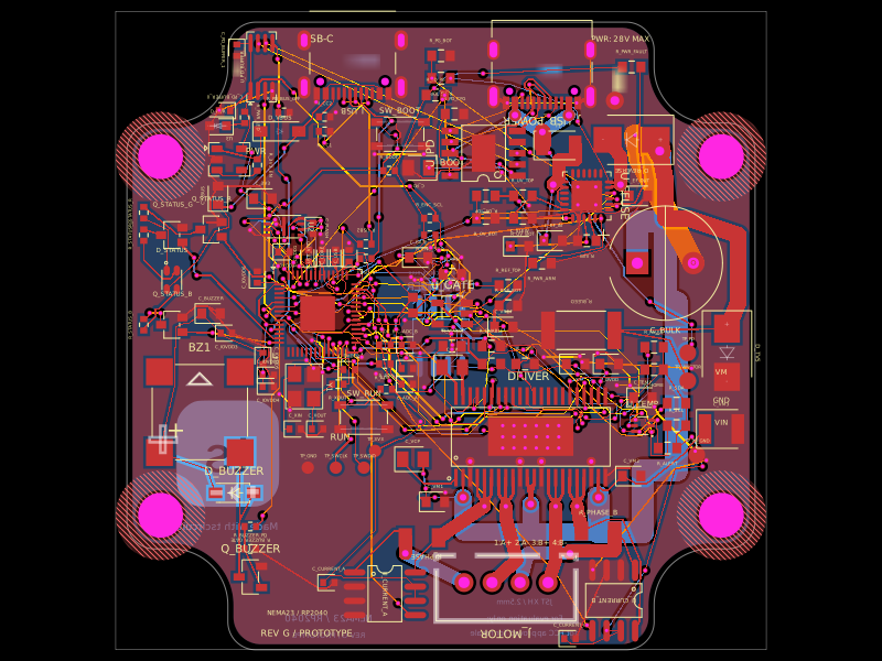 Discover something newimrishabh18/nema-23-stepper-controllerA curved NEMA23 rear-mount PCB combining an RP2040 controller, USB-C/USB-PD power input and protection, DRV8452 dual-winding stepper driver, current sensing, thermal interlock, status RGB LED, buzzer, and optional I²C encoder interface.