AnasSarkiz/magnetic-shutter-remote-r8
A USB‑C rechargeable battery-powered ESP32‑C3 wireless controller with Li‑ion charging, protected 3.3‑V buck‑boost regulation, thermal/safety monitoring, status LEDs, buttons, programming UART, crystal clock, and 2.4‑GHz antenna matching network.
- Version
- 0.4.0-prototype
- License
- unset
- Stars
- 0
scripts/write-r5-issues.py
"""Local blameless issue register; no network mutations."""
from pathlib import Path
ROOT=Path(__file__).resolve().parents[1]
issues=[
 ('045-independent-copper-reader-lacks-brep-regions','Independent checker cannot read native BREP copper pours','fixed locally','Project manufacturing audit / review reader; Gerbonara 1.5.0; Shapely 2.1.2','Project checker limitation, not a tscircuit defect',
  'scripts/manufacturing-audit.py and scripts/review-r3-exports.py accepted polygon/flash geometry only. R5 native copper pours emit BREP outer/inner rings and Gerber regions. The old reader raises Unsupported pour shape / Unsupported Gerber primitive rather than validating planes.',
  'tooling/gerber-review-venv/bin/python scripts/manufacturing-audit.py --input evidence/R5/grounding-first-routed/circuit.json --output evidence/R5/brep-reproduction.json\ntooling/gerber-review-venv/bin/python -m unittest discover -s tests -p test_curved_geometry.py -v',
  'Native circuit-json BREP schema: tooling/circuit-json/src/pcb/properties/brep.ts. Gerbonara ArcPoly.segments documents line/arc boundaries. Preserve holes and layer polarity; invalid rings must fail.',
  'Added scripts/curved_geometry.py with 0.000002 mm maximum chord sagitta; BREP bulges and Gerber arc centres are sampled independently. Polygon holes and clear polarity are retained. tests/test_curved_geometry.py covers empty holes, arc direction, independent circle agreement and invalid rings.',
  'evidence/R5/grounding-manufacturing-audit.log; tests/test_curved_geometry.py; scripts/curved_geometry.py'),
 ('046-parent-stencil-margin-cannot-style-imports','Parent stencil styling unavailable for immutable supplier footprints','fixed locally','@tscircuit/props 0.0.672 base f136fe4178b5b5ca80efb314b4fc3679ed068c61; @tscircuit/core 0.0.2035 base 3fcbb3842b8ab1c0af324078f6eb55c3dbcba1a0','Missing API capability, not supplier footprint corruption',
  'SmtPad supports a primitive solderPasteMargin but immutable imported JSX has no way for the parent to select individual aperture margins. pcbSx schema strips that unrecognised field. U2 lead default is 0.7 scaling: ~0.14×0.35 mm, area ratio ~0.40 at 0.125 mm.',
  'cd tooling/core\nbun test tests/components/primitive-components/smtpad-parent-paste-style.test.tsx',
  'The existing native solderPasteMargin means an absolute expansion per side; zero yields 1:1. Parent pcbSx styling must retain supplier copper unchanged. Declaration, defaults, accepted units and specificity are documented in tooling/props/lib/common/pcbSx.ts.',
  'Added typed unit-aware pcbSx solderPasteMargin with finite-value validation, plus SmtPad resolution. Explicit primitive props retain priority. EP-specific selector overrides the general lead margin. Source copper dimensions and 151 aperture count are tested; before implementation the test fails, after it passes. Native render snapshot is retained.',
  'evidence/R5/core-before-regressions.log; evidence/R5/core-after-regressions.log; tscircuit-issues/evidence/046-parent-stencil-style/SmtPad-before.ts; tscircuit-issues/evidence/046-parent-stencil-style/SmtPad-after.ts; tooling/patches/props-r5.patch; tooling/core/tests/components/primitive-components/__snapshots__/smtpad-parent-paste-style-pcb.snap.svg'),
 ('047-silkscreen-path-ignores-parent-visibility','Native silkscreen paths ignore inherited pcbSx visibility','fixed locally','@tscircuit/core 0.0.2035 local R3 attribution base 3fcbb3842b8ab1c0af324078f6eb55c3dbcba1a0; props 0.0.672','Confirmed core style integration inconsistency',
  'pcbSx visibility is parsed and inherited, and text respects hidden visibility; SilkscreenPath never resolves it and emits ornamental paths even when the parent selects hidden. This prevents source-controlled replacement of unprintable decorative artwork without touching imports.',
  'cd tooling/core\nbun test tests/components/primitive-components/silkscreen-path-parent-visibility.test.tsx',
  'Existing pcbSx visibility contract uses hidden/visible/inherit. Removing ornamental silk must leave electronic copper, courtyards, connectivity and models unchanged.',
  'SilkscreenPath resolves existing typed visibility before emitting. Before: two paths; after: one intended board path at 0.15 mm. Copper and courtyard counts are unchanged. Regression asserts emitted geometry and a native PCB snapshot.',
  'evidence/R5/core-before-regressions.log; evidence/R5/core-after-regressions.log; tscircuit-issues/evidence/047-silk-path-visibility/SilkscreenPath-before.ts; tscircuit-issues/evidence/047-silk-path-visibility/SilkscreenPath-after.ts; tooling/core/tests/components/primitive-components/__snapshots__/silkscreen-path-parent-visibility-pcb.snap.svg'),
 ('048-board-owned-silkscreen-fails-schema','Native board-level silkscreen has no valid schema owner','fixed locally','@tscircuit/core 0.0.2035; circuit-json 0.0.509 local sheet schema; exact local source/archives in tooling/revisions-r5.json','Confirmed core/schema integration defect',
  'A native board containing silkscreentext emits no pcb_component_id, while Circuit JSON requires a component owner. The native viewer displays it, but strict assembly/routed-schema consumers reject every board label. Representative exact schema error: pcb_silkscreen_text.pcb_component_id expected string, received undefined.',
  'cd tooling/core\nbun test tests/components/primitive-components/board-owned-silkscreen-schema.test.tsx\ncd ../circuit-json\nbun test tests/board-owned-silkscreen.test.ts',
  'Native board artwork is not an electronic component. It must reference the real board, while supplier artwork retains its component owner. Ownership must survive parsing; ownerless artwork must still be rejected.',
  'Schema accepts real pcb_board_id or pcb_component_id and requires at least one. Core emits board ownership for board artwork. No fake component IDs or electronic substitutes are introduced. Round-trip, ownerless rejection, component compatibility, emitted board IDs and visual regression are tested.',
  'evidence/R5/simplified-native-checks.log; evidence/R5/schema-silk-test.log; evidence/R5/schema-full-tests.log; evidence/R5/core-final-regressions.log; tooling/circuit-json/tests/board-owned-silkscreen.test.ts; tooling/core/tests/components/primitive-components/__snapshots__/board-owned-silkscreen-schema-pcb.snap.svg'),
 ('049-pour-npth-clearance-smaller-than-request','Requested pour clearance is smaller in actual NPTH copper geometry','suspected','@tscircuit/core 0.0.2035; @tscircuit/copper-pour-solver 0.0.62; circuit-json 0.0.509','Confirmed geometry discrepancy; responsible package/root cause not yet confirmed',
  'First R5 native pour configured 0.20 mm clearance. Independent actual BREP-to-circular-NPTH distances are 0.1968697634 and 0.1937395727 mm, below the 0.20 mm manufacturing requirement. No same-net or footprint exemption applies to NPTH.',
  'tooling/gerber-review-venv/bin/python scripts/manufacturing-audit.py --input evidence/R5/grounding-first-routed/circuit.json --output evidence/R5/npth-reproduction.json',
  'Selected JLC NPTH all-copper clearance is 0.20 mm: https://jlcpcb.com/capabilities/pcb-capabilities and https://jlcpcb.com/blog/npth-design-guide. The source request should not be represented as an actual measured clearance.',
  'Final native pour clearance is deliberately 0.30 mm and is independently rechecked. Manufacturing threshold remains 0.20. Whether polygonised NPTH obstacles/chord offsets in the pour solver produce the discrepancy is a hypothesis; no upstream fix is claimed. The project mitigation is not a package fix.',
  'evidence/R5/grounding-first-routed/circuit.json; evidence/R5/grounding-manufacturing-audit.json; evidence/R5/grounding-manufacturing-audit.log; evidence/R5/copper-audit.json'),
 ('050-usb-alternative-supplier-land-mismatches','Additional USB-C supplier libraries differ from manufacturer land drawings','confirmed','easyeda-converter 0.0.364 local R3 supported pipeline; raw supplier libraries C456012/C668623/C3151650','Supplier data discrepancies; not confirmed tscircuit converter bugs',
  'C456012 SHOU HAN TYPE-C 6P shell land is ~1.10×1.90 versus drawing 1.00×1.80. C668623 SHOU HAN TYPE-C 6P(073) CC land is ~0.70 versus drawing 0.90. C3151650 GCT USB4125-GF-A has 1.00 contact length versus A6 drawing 1.20, plus shell/drill differences. Exact raw dimensions are reproduced in R5 qualification.',
  'bun tooling/easyeda-converter/dist/main.cjs download -i C3151650 -o evidence/R5/C3151650.raweasy.json\npdftoppm -png -singlefile references/GCT-USB4125-current.pdf references/R5/GCT-USB4125-current',
  'Exact manufacturer recommended land patterns and explicit tolerances: references/R5/C456012.pdf, references/R5/C668623.pdf, references/GCT-USB4125-current.pdf (A6, 20/11/25). Manufacturer source: https://gct.co/connector/usb4125. Exact JLC listings: https://jlcpcb.com/partdetail/C456012 , https://jlcpcb.com/partdetail/C668623 , https://jlcpcb.com/partdetail/C3151650 .',
  'No supplier definition was altered and no candidate accepted. Import raw PAD dimensions reproduce the differing geometry before conversion, establishing supplier-model involvement. HCTL C2894893 remains blocked under issue 042. Exact supplier clarification is prepared, not sent.',
  'evidence/R5/C456012.raweasy.json; evidence/R5/C668623.raweasy.json; evidence/R5/C3151650.raweasy.json; references/R5/C456012.png; references/R5/C668623.png; references/R5/GCT-USB4125-current.png; R5-QUALIFICATION.md'),
 ('051-length-parser-accepts-nonfinite-invalid-unit','Length parser returns NaN for an invalid unit string','confirmed','circuit-json 0.0.509; @tscircuit/props 0.0.672','Confirmed unit parser behavior; broad upstream fix remains open',
  'Before adding a finite-value refinement, pcbSxValue.parse({solderPasteMargin:"invalid"}) returned solderPasteMargin: NaN instead of throwing. Exact failing assertion is preserved. This behavior is in the shared length parser and is not proof that fitted part geometry is invalid.',
  'cd tooling/props\nbun test tests/pcb-sx-solder-paste-margin.test.ts',
  'A physical stencil dimension must be finite or rejected. Native fanout source already uses positive/finite coordinate refinements; invalid physical input must not reach fabrication.',
  'The new paste-style API explicitly refines Number.isFinite and its regression rejects invalid units. This closes R5 stencil-input risk, not the shared parser defect in every consumer. No type escape or NaN fallback is used.',
  'evidence/R5/invalid-length-parser.log; tooling/props/tests/pcb-sx-solder-paste-margin.test.ts; evidence/R5/props-test.log; tooling/props/lib/common/pcbSx.ts'),
]
for slug,title,status,version,classification,actual,commands,expected,fix,evidence in issues:
 links=[]
 for f in evidence.split('; '):links.append(f'- [{f}](../{f})')
 text=f'''# {title}\n\nStatus: **{status}**. Classification: **{classification}**.\n\n## Affected package / exact revision\n\n{version}. Final archive hashes and source base revisions are in [R5 tooling manifest](../tooling/revisions-r5.json); original R4 imports and outputs remain protected.\n\n## Components and sources\n\nWhere applicable: TI BQ25185DLHR / C19725033, DLH0010A, [TI SLUSF65B](https://www.ti.com/lit/ds/symlink/bq25185.pdf), §7.4.1 and package/stencil examples. [Exact fitted identities](../bom.json). Additional USB identities/drawings are explicitly listed below. No fabricated electronic identity or footprint is introduced.\n\n## Minimal reproduction / commands / inputs\n\nRun from the R5 board directory unless the command explicitly changes directory:\n\n```sh\n{commands}\n```\n\nUse the preserved inputs linked below, the locked dependencies and supplied source. Network access is only needed to retrieve public supplier libraries; no account or upload is required.\n\n## Expected behavior\n\n{expected}\n\n## Actual behavior\n\n{actual}\n\n## Evidence / logs / geometry\n\n'''+ '\n'.join(links)+f'''\n\nBefore/after source, failing inputs and regression geometry are retained where applicable. No physical screenshot or physical test result is fabricated. Native/CAM views are generated evidence.\n\n## Root-cause findings\n\n{classification}. The actual behavior above is confirmed by the saved input/output. Any unconfirmed responsible-package or geometric approximation explanation is a hypothesis, explicitly identified. Import success is not manufacturer acceptance.\n\n## Impact\n\nCan affect strict schematic/PCB schema consumption, artwork, stencil generation or manufacturing geometry qualification. Scope is limited to the behavior reproduced above; it does not imply physical hardware failure or camera/RF compatibility.\n\n## Fix / changed files / regression / remaining blocker\n\n{fix}\n\nVerification results are in [R5 qualification summary](../evidence/R5/qualification-summary.json) and the exact linked regression logs. Do not interpret a local mitigation as verified upstream fixed. All reports are local; none was published.\n'''
 (ROOT/'tscircuit-issues'/(slug+'.md')).write_text(text)
index=ROOT/'tscircuit-issues/README.md';s=index.read_text();s=s.replace('magnetic shutter remote R4','magnetic shutter remote R5',1)
s+='\n## R5 additions\n\n| Issue | Affected package | Status | Classification |\n|---|---|---|---|\n'
for slug,title,status,version,classification,*_ in issues:s+=f'| [{slug} — {title}]({slug}.md) | {version} | {status} | {classification} |\n'
s+='\nR4 remains immutable in the source directory. Issue 043 regressions are retained. R5 closes the project grounding/legend gaps only after final actual-copper and export checks; issue 042 USB supplier qualification remains open. Physical validation is POST-PROTOTYPE PHYSICAL VALIDATION.\n';index.write_text(s)
Related Packages
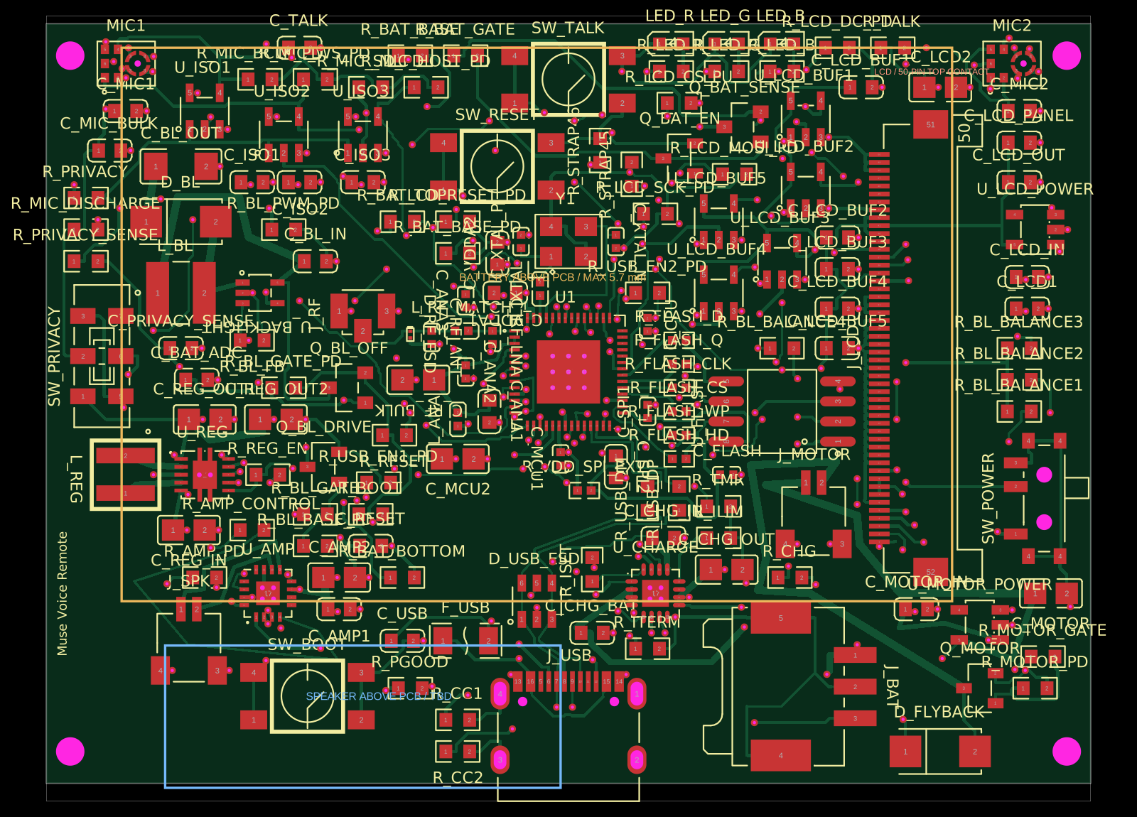 More from this authorAnasSarkiz/muse-voice-remoteMuse Voice Remote v1.3.0: checked prototype PCB/PCBA handoff. Bare ESP32-S3R8 chip, 155 TOP parts from 56 stocked JLCPCB imports with supplier CAD retained. Exact ER-TFT028A2-4 no-touch LCD, dual microphones, TALK, physical privacy, Wi-Fi, speaker, haptic and USB-C. Includes circuit.json, Gerbers/drills, JLC BOM/CPL, segmented stencil artwork and 19 filled/capped thermal-hole map. Native/factory DRC clean; 20 tests pass. See manufacturing/FABRICATION-NOTES.md for stackup and assembly requirements. Physical device/enclosure/RF qualification, firmware and connected-service MUSE integration remain unverified.
 Similar packageaura/diy-power-delivery-triggerThis hardware design implements a USB Type-C port with supporting power management and signal conditioning components, including a USB-C connector, a FUSB302 USB-C port controller, ESD protection diodes, a buck converter for 3.3V power regulation, an STM32 microcontroller for control and processing, an RGB LED indicator, push button, terminal block connections, and associated filtering and support components.
 Discover something newseveibar/am3352-ram-dogbone-and-single-layer-route-testAM3352BZCZ100 processor connected to a W631GG6MB-12 DDR3 memory chip through a routed, length-matched 16-bit DDR interface with clock/data-strobe pairs and control/address signals.