AnasSarkiz/magnetic-shutter-remote-r8
A USB‑C rechargeable battery-powered ESP32‑C3 wireless controller with Li‑ion charging, protected 3.3‑V buck‑boost regulation, thermal/safety monitoring, status LEDs, buttons, programming UART, crystal clock, and 2.4‑GHz antenna matching network.
- Version
- 0.4.0-prototype
- License
- unset
- Stars
- 0
scripts/review-r8-process.py
"""Measure the actual R8 CAM process features; never modify manufacturing files."""
import argparse
import importlib.util
import json
import math
import hashlib
import subprocess
import sys
from pathlib import Path
from zipfile import ZipFile

from gerbonara import GerberFile
from shapely.geometry import LineString, box
from shapely.ops import polygonize, unary_union

ROOT = Path(__file__).resolve().parents[1]


def label_overlap_failures(labels):
    failures = []
    for i, first in enumerate(labels):
        for second in labels[:i]:
            if first['layer'] != second['layer']:
                continue
            overlap = box(*first['bounds_mm']).intersection(box(*second['bounds_mm'])).area
            if overlap > 1e-8:
                failures.append({'rule':'functional_legend_overlap',
                                 'texts':[first['text'],second['text']],
                                 'layer':first['layer'], 'bounding_overlap_mm2':overlap})
    return failures


def load(name, filename):
    spec = importlib.util.spec_from_file_location(name, ROOT/'scripts'/filename)
    module = importlib.util.module_from_spec(spec)
    sys.modules[name] = module
    spec.loader.exec_module(module)
    return module


GEOMETRY = load('r8_process_geometry', 'manufacturing-audit.py')
READER = load('r8_process_reader', 'review-r3-exports.py')


def release_metrics(geometry, thickness):
    if not geometry.is_valid or geometry.area <= 0 or thickness <= 0:
        raise ValueError('Invalid stencil geometry or thickness')
    points = list(geometry.convex_hull.exterior.coords)
    widths = []
    for a, b in zip(points, points[1:]):
        dx, dy = b[0]-a[0], b[1]-a[1]
        length = math.hypot(dx, dy)
        if not length:
            raise ValueError('Degenerate aperture edge')
        projections = [(-dy*x+dx*y)/length for x, y in points[:-1]]
        widths.append(max(projections)-min(projections))
    return {'area_ratio': geometry.area/(geometry.length*thickness),
            'aspect_ratio': min(widths)/thickness}


def silkscreen_metrics(layer, geometry, mask, outline):
    """Measure all exported silk, including supplier circles and paths."""
    strokes = [p.width for obj in layer.objects for p in obj.to_primitives() if hasattr(p,'width')]
    if not geometry.is_empty and not strokes:
        raise ValueError('Nonempty silkscreen has no supported measurable strokes')
    return {'minimum_stroke_mm':min(strokes) if strokes else None,
            'mask_gap_mm':None if geometry.is_empty or mask.is_empty else geometry.distance(mask),
            'outside_outline_mm2':geometry.difference(outline).area}


def attribute_paste(geometry, context):
    """Assign by actual copper contact, permitting intentionally asymmetric paste.
    Every aperture must contact exactly one fitted land, belong to its component,
    and remain inside actual exported mask openings. Centroid equality is not a
    physical requirement for a reduced/asymmetric manufacturer aperture.
    """
    contacts = [land for land in context['lands'] if land.layer == context['layer']
                and land.geometry.intersection(geometry).area > GEOMETRY.EPS**2]
    if len(contacts) != 1 or contacts[0].owner != context['owner']:
        raise ValueError('Paste aperture does not contact exactly one owned land')
    if not context['mask'].buffer(READER.COPPER_COMPARE_MM).covers(geometry):
        raise ValueError('Paste aperture extends outside actual solder-mask openings')
    return contacts[0]


def review(args):
    circuit = json.loads(args.circuit.read_text())
    args.output.mkdir(parents=True, exist_ok=True)
    names = {e['source_component_id']: e['name'] for e in circuit if e['type']=='source_component'}
    owners = {e['pcb_component_id']: names[e['source_component_id']] for e in circuit
              if e['type']=='pcb_component' and e['source_component_id'] in names}
    pads = {e['pcb_smtpad_id']: e for e in circuit if e['type']=='pcb_smtpad'}
    copper, _, _ = GEOMETRY.make_features(circuit, 'gerber')
    lands = [f for f in copper if f.kind == 'smt' or (f.kind == 'annulus' and f.owner)]
    if any(f.owner not in owners for f in lands):
        raise ValueError('A fitted CAM terminal has no verified source component')
    paste_coverage = set()
    with ZipFile(args.archive) as archive:
        layers = {name: GerberFile.from_string(archive.read(name).decode()) for name in
                  ['F_Mask.gbr', 'B_Mask.gbr', 'F_SilkScreen.gbr', 'B_SilkScreen.gbr', 'Edge_Cuts.gbr']}
    masks = {side: READER.copper_geometry(layers[name]) for side, name in [('top','F_Mask.gbr'),('bottom','B_Mask.gbr')]}
    silks = {side: READER.copper_geometry(layers[name]) for side, name in [('top','F_SilkScreen.gbr'),('bottom','B_SilkScreen.gbr')]}
    lines = [LineString([(p.x1,p.y1),(p.x2,p.y2)]) for obj in layers['Edge_Cuts.gbr'].objects for p in obj.to_primitives()]
    outlines = list(polygonize(unary_union(lines)))
    if len(outlines) != 1:
        raise ValueError('Unsupported or open board outline')
    outline = outlines[0]
    failures, stencil, webs, labels = [], [], [], []
    complete_silk = {}
    for side, filename in [('top','F_SilkScreen.gbr'),('bottom','B_SilkScreen.gbr')]:
        row = silkscreen_metrics(layers[filename],silks[side],masks[side],outline)
        complete_silk[side] = row
        if (row['minimum_stroke_mm'] is not None and row['minimum_stroke_mm'] < .15) or (row['mask_gap_mm'] is not None and row['mask_gap_mm'] < .15 + GEOMETRY.EPS) or row['outside_outline_mm2'] > GEOMETRY.EPS**2:
            failures.append({'rule':'complete_silkscreen','layer':side,**row})
    for paste in (e for e in circuit if e['type']=='pcb_solder_paste'):
        geometry = GEOMETRY.pad(paste)
        row = {'id':paste['pcb_solder_paste_id'], 'ref':owners[paste['pcb_component_id']], **release_metrics(geometry,.1)}
        land = attribute_paste(geometry, {'lands':lands,'owner':paste['pcb_component_id'],
                                        'layer':paste['layer'],'mask':masks[paste['layer']]})
        row['land'] = land.id
        row['coverage_percent'] = 100*geometry.area/land.geometry.area
        paste_coverage.add(land.id)
        stencil.append(row)
        if row['area_ratio'] < .66 or row['aspect_ratio'] < 1.5:
            failures.append({'rule':'stencil_release', **row})
    if paste_coverage != {f.id for f in lands if f.layer == 'top'}:
        failures.append({'rule':'stencil_pad_coverage'})
    for side, filename in [('top','F_Mask.gbr'),('bottom','B_Mask.gbr')]:
        flashes = [READER.copper_geometry(GerberFile(objects=[obj])) for obj in layers[filename].objects]
        contacts = []
        for pad in (p for p in pads.values() if p['layer']==side):
            pad_centroid = GEOMETRY.pad(pad).centroid
            matches = [g for g in flashes if g.centroid.distance(pad_centroid)<.000002]
            if len(matches) != 1:
                raise ValueError(f'Mask opening not uniquely attributable: {pad["pcb_smtpad_id"]}')
            contacts.append((pad, matches[0]))
        for i, (first, a) in enumerate(contacts):
            for second, b in contacts[:i]:
                gap = a.distance(b)
                if gap < .3:
                    row = {'pads':[first['pcb_smtpad_id'],second['pcb_smtpad_id']],
                           'refs':[owners[first['pcb_component_id']],owners[second['pcb_component_id']]],
                           'layer':side,'gap_mm':gap}
                    webs.append(row)
                    if gap < .1 + GEOMETRY.EPS:
                        failures.append({'rule':'mask_web', **row})
    board = next(e for e in circuit if e['type']=='pcb_board')
    isolated = args.output/'isolated-labels'
    isolated.mkdir(exist_ok=True)
    for text in (e for e in circuit if e['type']=='pcb_silkscreen_text'):
        path = isolated/(text['pcb_silkscreen_text_id']+'.json')
        # Read-only isolated attribution, never used as fabrication input.
        path.write_text(json.dumps([board,text],indent=2)+'\n')
        archive_path = path.with_suffix('.zip')
        subprocess.run(['bun','node_modules/circuit-json-to-gerber/dist/cli.js',str(path),'-o',str(archive_path)],cwd=ROOT,check=True,capture_output=True)
        with ZipFile(archive_path) as archive:
            layer = GerberFile.from_string(archive.read('F_SilkScreen.gbr' if text['layer']=='top' else 'B_SilkScreen.gbr').decode())
        geometry = READER.copper_geometry(layer)
        if not silks[text['layer']].buffer(READER.COPPER_COMPARE_MM).covers(geometry):
            raise ValueError('Attributed legend missing from full actual export')
        strokes = [p.width for obj in layer.objects for p in obj.to_primitives() if hasattr(p,'width')]
        row = {'text':text['text'],'layer':text['layer'],'bounds_mm':geometry.bounds,
               'minimum_stroke_mm':min(strokes),'mask_gap_mm':geometry.distance(masks[text['layer']]),
               'outside_outline_mm2':geometry.difference(outline).area}
        labels.append(row)
        if row['minimum_stroke_mm'] < .15 or row['mask_gap_mm'] < .15 + GEOMETRY.EPS or row['outside_outline_mm2'] > GEOMETRY.EPS**2:
            failures.append({'rule':'silkscreen', **row})
    failures.extend(label_overlap_failures(labels))
    for hole in (e for e in circuit if e['type'] in ('pcb_via','pcb_plated_hole','pcb_hole')):
        size = hole.get('hole_diameter',min(hole.get('hole_width',math.inf),hole.get('hole_height',math.inf)))
        minimum = .3 if hole['type']=='pcb_via' else .5
        if size < minimum:
            failures.append({'rule':'drill_size','feature':hole,'minimum_mm':minimum})
    report = {'circuit_sha256':hashlib.sha256(args.circuit.read_bytes()).hexdigest(),'archive_sha256':hashlib.sha256(args.archive.read_bytes()).hexdigest(),'failures':failures,'stencil_thickness_mm':.1,'stencil':stencil,'mask_webs':sorted(webs,key=lambda r:r['gap_mm']),
              'labels':labels,'complete_silkscreen':complete_silk,'references':['https://jlcpcb.com/capabilities/pcb-capabilities','TI SLUA271C sections 4.2–4.4'],
              'limitations':['Nominal process geometry only; no assembly approval, measured paste transfer or supplier processed-preview is claimed.']}
    (args.output/'process-review.json').write_text(json.dumps(report,indent=2,allow_nan=False)+'\n')
    print('Stencil apertures:',len(stencil),'minimum area ratio:',min(r['area_ratio'] for r in stencil),'mask web minimum:',min(r['gap_mm'] for r in webs),'process failures:',len(failures))
    for failure in failures:print(failure)
    return bool(failures)


if __name__=='__main__':
    parser = argparse.ArgumentParser()
    parser.add_argument('archive',type=Path)
    parser.add_argument('circuit',type=Path)
    parser.add_argument('--output',type=Path,required=True)
    raise SystemExit(review(parser.parse_args()))
Related Packages
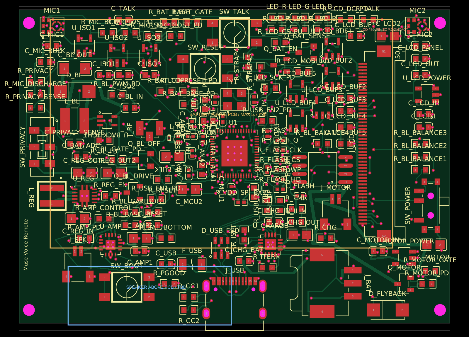 More from this authorAnasSarkiz/muse-voice-remoteMuse Voice Remote v1.3.0: checked prototype PCB/PCBA handoff. Bare ESP32-S3R8 chip, 155 TOP parts from 56 stocked JLCPCB imports with supplier CAD retained. Exact ER-TFT028A2-4 no-touch LCD, dual microphones, TALK, physical privacy, Wi-Fi, speaker, haptic and USB-C. Includes circuit.json, Gerbers/drills, JLC BOM/CPL, segmented stencil artwork and 19 filled/capped thermal-hole map. Native/factory DRC clean; 20 tests pass. See manufacturing/FABRICATION-NOTES.md for stackup and assembly requirements. Physical device/enclosure/RF qualification, firmware and connected-service MUSE integration remain unverified.
 Similar packageaura/diy-power-delivery-triggerThis hardware design implements a USB Type-C port with supporting power management and signal conditioning components, including a USB-C connector, a FUSB302 USB-C port controller, ESD protection diodes, a buck converter for 3.3V power regulation, an STM32 microcontroller for control and processing, an RGB LED indicator, push button, terminal block connections, and associated filtering and support components.
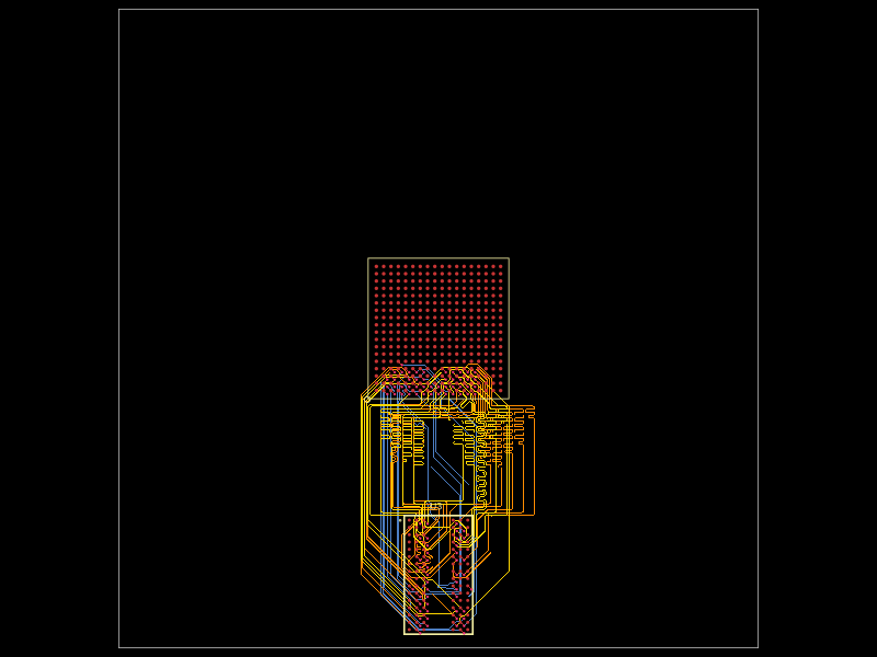 Discover something newseveibar/am3352-ram-dogbone-and-single-layer-route-testAM3352BZCZ100 processor connected to a W631GG6MB-12 DDR3 memory chip through a routed, length-matched 16-bit DDR interface with clock/data-strobe pairs and control/address signals.