AnasSarkiz/magnetic-shutter-remote-r8
A USB‑C rechargeable battery-powered ESP32‑C3 wireless controller with Li‑ion charging, protected 3.3‑V buck‑boost regulation, thermal/safety monitoring, status LEDs, buttons, programming UART, crystal clock, and 2.4‑GHz antenna matching network.
- Version
- 0.4.0-prototype
- License
- unset
- Stars
- 0
scripts/measure-j1-export.py
"""Independent R2 J1 metrology from original Gerber flashes and NPTH drills.
Board Cartesian XY millimetres. Gerber rotation is handled in the pad frame.
No Circuit JSON geometry is used to compute the exported gap.
"""
import json,math,zipfile
from pathlib import Path
from gerbonara import GerberFile,ExcellonFile
from gerbonara.graphic_objects import Flash
from gerbonara.apertures import RectangleAperture
r=Path('evidence/R3/R2-export-metrology');r.mkdir(exist_ok=True)
with zipfile.ZipFile('evidence/R3/R2-inputs/fabrication/R2-gerbers-review.zip') as z:z.extractall(r)
cu=GerberFile.open(r/'F_Cu.gbr');drill=ExcellonFile.open(r/'drill_npth.drl')
rects=[p for p in cu.objects if isinstance(p,Flash) and isinstance(p.aperture,RectangleAperture)]
records=[]
for hole in drill.objects:
if not (abs(abs(hole.x)-2.89)<.001 and abs(hole.y-22.9601)<.001):continue
nearest=[]
for p in rects:
# Gerbonara exposes aperture rotation in radians (0 for these rectangles).
angle=getattr(p.aperture,'rotation',0) or 0
dx,dy=hole.x-p.x,hole.y-p.y
lx=dx*math.cos(angle)+dy*math.sin(angle);ly=-dx*math.sin(angle)+dy*math.cos(angle)
cx=min(max(lx,-p.aperture.w/2),p.aperture.w/2);cy=min(max(ly,-p.aperture.h/2),p.aperture.h/2)
gap=math.hypot(lx-cx,ly-cy)-hole.tool.diameter/2
corner=(p.x+cx*math.cos(angle)-cy*math.sin(angle),p.y+cx*math.sin(angle)+cy*math.cos(angle))
nearest.append((gap,p,corner,angle))
gap,p,corner,angle=min(nearest,key=lambda a:a[0])
records.append({'source_hole_id':'pcb_hole_1' if hole.x>0 else 'pcb_hole_0','source_pad_id':'pcb_smtpad_2' if hole.x>0 else 'pcb_smtpad_0','reference':'J1','terminal':'pin7 / GND2' if hole.x>0 else 'pin5 / GND1','hole':{'x':hole.x,'y':hole.y,'diameter':hole.tool.diameter},'pad':{'x':p.x,'y':p.y,'width':p.aperture.w,'height':p.aperture.h,'rotation_radians':angle},'nearest_copper_point':corner,'clearance_mm':gap,'threshold_mm':.2,'manufacturer_nominal_mm':math.hypot(.01,.5)-.325,'source_clearance_mm':.17528138222899436 if hole.x>0 else math.hypot(.0101346,.5001768)-.324993})
assert len(records)==2
Path('evidence/R3/j1-export-metrology.json').write_text(json.dumps(records,indent=2)+'\n')
# Engineering SVG, derived only from the parsed exported geometry.
S=260;ox=160;oy=90;cx=records[1 if records[1]['hole']['x']>0 else 0] if records[0]['hole']['x']<0 else records[0]
h=cx['hole'];p=cx['pad'];near=cx['nearest_copper_point']
x=lambda v:ox+(v-2.2)*S;y=lambda v:oy+(23.6-v)*S
out=['<svg xmlns="http://www.w3.org/2000/svg" width="1050" height="700" viewBox="0 0 1050 700">','<rect width="1050" height="700" fill="white"/>','<g font-family="sans-serif" fill="#142b38">','<text x="40" y="34" font-size="22">R2 J1: independent Gerber + NPTH measurement</text>','<text x="40" y="62" font-size="15">Original exported files; board XY mm; magnified drawing, dimensions govern</text>']
for pp in rects:
if 1.9<pp.x<3.6 and 21.5<pp.y<22.2:
out.append(f'<rect x="{x(pp.x-pp.aperture.w/2)}" y="{y(pp.y+pp.aperture.h/2)}" width="{pp.aperture.w*S}" height="{pp.aperture.h*S}" fill="#cb9d39" stroke="#624913"/>')
out.append(f'<circle cx="{x(h["x"])}" cy="{y(h["y"])}" r="{h["diameter"]/2*S}" fill="#ebf3f8" stroke="#253f52" stroke-width="2"/>')
ux=(near[0]-h['x']);uy=(near[1]-h['y']);d=math.hypot(ux,uy);start=(h['x']+ux/d*h['diameter']/2,h['y']+uy/d*h['diameter']/2)
out.extend([f'<line x1="{x(start[0])}" y1="{y(start[1])}" x2="{x(near[0])}" y2="{y(near[1])}" stroke="#c52526" stroke-width="5"/>',f'<circle cx="{x(near[0])}" cy="{y(near[1])}" r="4" fill="#c52526"/>',f'<text x="610" y="155" font-size="18">Right locator: pcb_hole_1</text>',f'<text x="610" y="184" font-size="16">X {h["x"]:.4f}, Y {h["y"]:.4f}; Ø {h["diameter"]:.6f}</text>',f'<text x="610" y="241" font-size="18">Nearest copper: pcb_smtpad_2</text>',f'<text x="610" y="270" font-size="16">J1 pin7 / GND2; rectangular pad</text>',f'<text x="610" y="299" font-size="16">{p["width"]:.6f} × {p["height"]:.6f}; rotation {math.degrees(p["rotation_radians"]):.0f}°</text>',f'<text x="610" y="357" font-size="23" fill="#c52526">Gap {cx["clearance_mm"]:.6f} mm < 0.200 mm</text>','<text x="610" y="391" font-size="15">Gap is to the corner, not the pad bounding centre.</text>','<text x="40" y="586" font-size="16">Symmetric left locator also fails against J1 pin5 / GND1; see measurement JSON.</text>','<text x="40" y="616" font-size="16">GCT nominal land geometry: 0.175100 mm. Source: 0.175281 mm.</text>','<text x="40" y="646" font-size="15">JLCPCB NPTH design guide: 0.2–0.3 mm clearance to copper. No same-footprint exemption.</text>','</g></svg>'])
Path('evidence/R3/j1-clearance-annotated.svg').write_text('\n'.join(out))
print(json.dumps(records,indent=2))
Related Packages
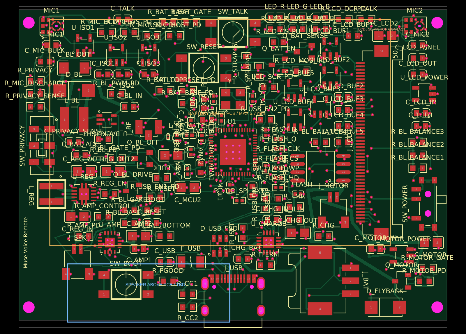 More from this authorAnasSarkiz/muse-voice-remoteMuse Voice Remote v1.3.0: checked prototype PCB/PCBA handoff. Bare ESP32-S3R8 chip, 155 TOP parts from 56 stocked JLCPCB imports with supplier CAD retained. Exact ER-TFT028A2-4 no-touch LCD, dual microphones, TALK, physical privacy, Wi-Fi, speaker, haptic and USB-C. Includes circuit.json, Gerbers/drills, JLC BOM/CPL, segmented stencil artwork and 19 filled/capped thermal-hole map. Native/factory DRC clean; 20 tests pass. See manufacturing/FABRICATION-NOTES.md for stackup and assembly requirements. Physical device/enclosure/RF qualification, firmware and connected-service MUSE integration remain unverified.
 Similar packageaura/diy-power-delivery-triggerThis hardware design implements a USB Type-C port with supporting power management and signal conditioning components, including a USB-C connector, a FUSB302 USB-C port controller, ESD protection diodes, a buck converter for 3.3V power regulation, an STM32 microcontroller for control and processing, an RGB LED indicator, push button, terminal block connections, and associated filtering and support components.
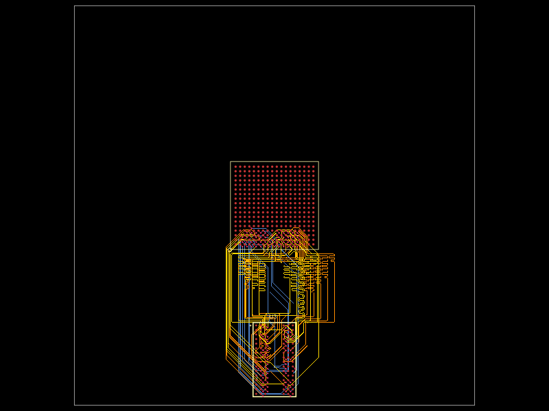 Discover something newseveibar/am3352-ram-dogbone-and-single-layer-route-testAM3352BZCZ100 processor connected to a W631GG6MB-12 DDR3 memory chip through a routed, length-matched 16-bit DDR interface with clock/data-strobe pairs and control/address signals.